Seabed Delay Major Sound DRop

l_elu

Member
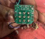
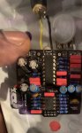
Hello All, so where do I even begin this is gonna be a interesting one, hopefully we can trouble shoot it. I created the Seabed Delay Pedal, got it all boxed up but forgot to actually solder the stomp to the stomp pcb but everything else was connected. When the guitar is in bypass mode I get a full bypass guitar sound, and moving the pot controls does nothing. when I go ahead and activate the pedal, the volume drops to like 20%. All the controls still work for the effects it seems like they are just operating at 20%. If I crank the amp all the way up it gives me a beautiful delay that I would love to play around with, I just don't want to deactivate the pedal and the roof come off my house from having the amp cranked full blast.
On to the trouble shooting, so I went around and tried to re-solder most spots that I cant access. I replaced both ic chips and the transistor. nothing. So then i went and double checked all the resistors and all matched the value that the pcb called for. Double checked all the caps that were not sandwiched together( I always try and put the identification number on the outside) looks like they are correct but haven't confirmed all. Next step was to get all the reading:
IC2 PT2399
Pin 1: 4.92
Pin 2: 2.48
Pin 3: 0
Pin 4: .02
Pin 5: 2.57
Pin 6: 2.49
Pin 7: .28
Pin 8: .87
Pin 9: 2.49
Pin 10: 2.49
Pin 11: 2.49
Pin 12: 2.49
Pin 13: 2.49
Pin 14: 2.49
Pin 15: 2.49
Pin 16: 2.49


IC1 TL072
Pin 1: 4.10
Pin 2: 4.10
Pin 3: 4.08
Pin 4: 0
Pin 5: 8.20
Pin 6: 4.10
Pin 7: 4.10
Pin 8: 4.08

IC3 78L05
Pin 1: 8.20
Pin 2: 0
Pin 3: 4.98
 
Last edited:
Your voltages for the TL072 look OK if you have mis-numbered the pins. One of the easiest ways to track down a volume drop is to make an audio probe and probe through the audio path of the circuit until you find where it gets quiet. If you google audio probe you will find out how to make one and use it.
 
Yeah lol the other 2 were consistent with the right side measuring at 2.49. So I made the audio probe and that’s the main reason I’m hear. I don’t know what I’m looking for here. Am I supposed to hear the effect or is it just like and active pickup type sounds!?!?
 
So with the audio probe you basically need to follow through the audio path until you hear a large drop in volume. Looking at the schematic for this circuit, the path is: C1 -> R2 -> IC1 Pin 2 -> IC1 pin 1 -> R4 -> IC1 pin 6 -> ic1 pin 7 -> C4 -> R6. That is for the clean unaffected sound. Given that you have a big volume drop it sounds as if this pathway has a problem, but if there is no problem in that path then look at the delay signal. If you are not getting anything at pins 15 and 16 then you are not getting any sound to the input of the chip, so you will not be getting any delay. check for audio around C5, R7, R8, R9 and C7
 
So I tested it in bypass cause I wasn’t getting a sound(when I strum the guitar I could hear the cords) it was just connecting you the signal(clean noise as if it’s connected to ground) if that makes sense. I got R1,R2,R3,C2,R7,C14,level B50k,C13,R14.
No sound on:ic1,R14,R5,R15,C4,R6,R10,R17,delay B50k,D1 ,Ic3,C22

honestly I don’t think I getting anything once I’m in effect mode. Is it the switch?
 
If you have the pedal in effect on switch position (not bypass) and you are getting sound at the junction of R1 and C1 then your switch is letting the sound get through to the board. If it is not getting through to IC1 from there, the the problem has to be either C1, R2 or one of the solder connections around those components. Check for bad solder joints or solder bridges around there.
 
No sound in neither R1 or C1. I really took a good look at it and it seemed like there was a little short from one of the stranded wires connecting to another leg but that wasn’t it either. I need help!!!! Could it be that there something wrong with the foot switch. I hit its lugs all around to make sure they were good and checked the bottom.I’m slumped I have to be missing something here.....
 
here’s some pictures on my broken screen.
 

Attachments

  • 34DFF935-CD30-45CB-AB70-C7785B6EB959.jpeg
    34DFF935-CD30-45CB-AB70-C7785B6EB959.jpeg
    82.3 KB · Views: 12
  • AE755E96-DF95-4B3C-A98D-1C4CC12736E4.jpeg
    AE755E96-DF95-4B3C-A98D-1C4CC12736E4.jpeg
    88 KB · Views: 13
  • 40031AB3-E7BC-4CA0-A6C1-037D4E745B73.jpeg
    40031AB3-E7BC-4CA0-A6C1-037D4E745B73.jpeg
    69.3 KB · Views: 12
  • C596393F-E153-405B-942D-EF4F63B6AFB5.jpeg
    C596393F-E153-405B-942D-EF4F63B6AFB5.jpeg
    88 KB · Views: 11
  • 77473C26-FA27-48B4-B20F-691CC4313DC2.jpeg
    77473C26-FA27-48B4-B20F-691CC4313DC2.jpeg
    79.6 KB · Views: 12
  • 3AC97231-D2C6-4A19-A0DD-FAC7F6FE64FD.jpeg
    3AC97231-D2C6-4A19-A0DD-FAC7F6FE64FD.jpeg
    91.1 KB · Views: 13
  • BC2AC37D-3D3E-4644-A52F-68677EFCD0AE.jpeg
    BC2AC37D-3D3E-4644-A52F-68677EFCD0AE.jpeg
    110.6 KB · Views: 13
  • F7744924-382C-47F0-A39A-1B4F50FDB572.jpeg
    F7744924-382C-47F0-A39A-1B4F50FDB572.jpeg
    68.2 KB · Views: 12
  • C251DC7D-2CCC-4251-8A3C-49FE067834A8.jpeg
    C251DC7D-2CCC-4251-8A3C-49FE067834A8.jpeg
    101.4 KB · Views: 11
  • E658BDEC-77D1-45C9-BB9E-69815B62F7EE.jpeg
    E658BDEC-77D1-45C9-BB9E-69815B62F7EE.jpeg
    110.1 KB · Views: 11
What are all the steps I should check from where we’re at, I just need someone to start from.../ I saw another topic in a forum where someone asked if the host was using NP
Electrolytic capacitors. Is that a problem on these builds.
 
2 things to check next. One is to make sure that you have plugged the guitar and amp into the correct jacks. It is very easy to mix up the input and output jacks when it is upside down and out of the box. If you do that of course bypass will work, but the effect won't. Next thing to check is indeed the switch. These switches are pretty sensitive to heat and can be damaged during the soldering process. You need to be quick and precise and take a break between pins to let it cool. Do you know how to use your multimeter to measure continuity? If so then measure the switch pins for continuity without any power to the circuit. There is a line of pins in the middle that will connect to one side or the other depending on which position the switch is in. Measure and make sure the middle pins are all connected to the same side. Then switch the switch, and they all should connect to the other side instead. I usually check that a few times just to make sure. If that is all correct then your switch is OK. If some of the pins don't switch from side to side then you will need a new switch.
 
This is the results of the continuity test. Yellow are connections when effect is on.
 

Attachments

  • DA92C626-7717-4900-838A-B012C48ED6E2.jpeg
    DA92C626-7717-4900-838A-B012C48ED6E2.jpeg
    997.7 KB · Views: 9
This is what you should be looking for - continuity of the switch lugs, not continuity with the PC board. It looks like only the middle one is working as it should? If this is the case then you need a new switch, but before you replace it, test as per this diagram.
1601343128260.png
 
1,4,7 connect we’ll with my solder points. Solder points 2,8 connect well with 3,9 but 5,6 only connect at the lug(not the solder point for some reason)
 
Last edited:
So, let me just check and make sure I am understanding you.

With the switch in one position, 1 connects to 2, 4 connects to 5, 7 connects to 8 and all of them connect well to the solder points on the board.

With the switch in the other position, 2 connects to 3, 8 connects to 9 and these connect to the board well. 5 connects to 6 but there is no connection to the board?

If I have understood you correctly then try lug 6 looks suspicious, so reflow the solder on that lug (although your soldering looks very good, so I doubt that is the problem). If that does not work then try soldering a short lead from lug 6 of the switch to the pad that it is supposed to connect to, as you might have a broken track on the board.

I have just looked again at your photo of the board, and I think the middle bank is for switching the LED. It is hard to tell without seeing the traces on the other side but I have marked what I think is happening on this board.

1601346952228.png

We know that bypass works, so that would mean that all the connections on the bottom row are OK, and the middle row is OK. We need to make sure that when the effect is engaged that the middle left lug connects properly to the upper left lug, and the middle right lug connects to the upper right lug (2 to 1 and 8 to 7 on the above drawing). 1 to 2 is what would stop sound getting to your delay board if it was broken. I think you said that all these connections do in fact work? If so then check continuity from the BI pad on the switch PCB with lug 1, and then also check the BI pad with the delay board input.
 
So there is continuity between Bi and lug 1. I and lug 2. Bo and lug 7. G and lug 5 and 6. In (on the seabed pcb) and Bi(only) Out( on the seabed pcb) BO.

G and lug 4,5. Bo and lug 7. O and lug 9,8,3,2, .I and lug 3,2,8,9.
In both positions lug 3 and 9 are always connected.

Sorry for the late response.
 
Last edited:
OK, this is not making too much sense to me. Try with the audio probe again. With the switch set to "effect on" check for audio in this order: Tip of the input jack, I pad on the switch board, Lug 2 of the switch, lug 1 of the switch, BI pad on the switch board, the input pad of the delay board. The next step is C1, and we already know it's not getting that far.
 
Quick question? Well I get a signal path in this region when testing with an audio probe.
 

Attachments

  • 517038AB-23FA-4D8D-9B55-310FB26562C1.jpeg
    517038AB-23FA-4D8D-9B55-310FB26562C1.jpeg
    45.3 KB · Views: 8
Back
Top