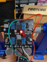
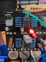
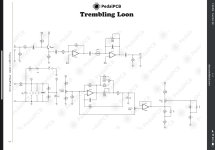
SW/GND at the four solder pads at the bottom is just for the bypass LED. He's using the audio jack daughter board, which is connected, but the connection at the black wire looks like a garbage fire
When you solder wires, do it by stripping 1/4" of insulation off, then twist the strands together to give them strength, then tin the bare wire, which means touch your soldering iron to it to heat it up and then introduce a small amount of solder such that it wicks to and coats the wires. Then put this thru the solder pad and introduce more solder along with heat to the joint. Once it's done trim off the excess. Clean it all up this way and be sure to pay attention to the finer details.
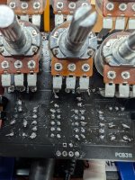
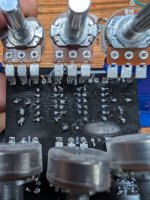
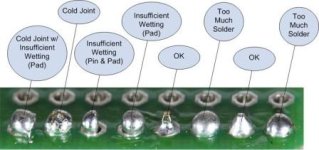
Also your solder joints at the pots esp look cold. You want to turn up your iron to like 750F, or almost all the way, and heat the components for a few secs before introducing solder to the heated components. Then remove the heat once the solder has wicked onto the metal surfaces. The blob shapes on your joints mean the solder wasn't able to flow properly, which means it's not hot enough. You should be able to see the molten solder develop surface tension like water does.
When you solder IC's, you want to use sockets because it makes it 100x easier to remove the IC if there is a problem. Also, it's important to jump around from different pins so you don't concentrate too much heat in one area. The problem you're having where pin 2 of IC1 isn't passing signal could be due to an overheated IC.


