UN-inverting an inverting boost.

like Yeah!

Active member
edit- The originally intended question should have been about how to wire the given breakout circuit to another circuit to invert it on the input, but only when the pedal is active... so it would remain true bypass. the related corrected image is here at post #13. Living and learning is the spice

TL;DR: til that jfet buffers are not jfet boosts, and also that @Robert is a great human being.

Hi. I've read that single fet boosts invert the input signal.. and a way to uninvert it is to just use a single fet buffer along with it.
so i saw the jfet buffer board and i got one along with the fumble board ..for science!
i read in the docs for the buffer that it's literally a raw buffer and power protection/filtering are to be addressed by the installer (me).

Is this an acceptable way to provide power to the buffer board and connect it to the circuit as an input inverter that can be switched out of circuit?

[images removed (they were bad anyway)]
 
Last edited:
If you want an "inverting buffer," you can build it on a SHO PCB.

Replace the mosfet with a JFET and the boost control with a fixed resistor equal to the drain resistor.
 
If you want an "inverting buffer," you can build it on a SHO PCB.

Replace the mosfet with a JFET and the boost control with a fixed resistor equal to the drain resistor.
i don't even really want the idea of a buffer in the circuit, i was just thinking to make what's already present ...invertable..
i just mistakenly thought a jfet buffer was the same as a jfet boost, but with gain of 1.
i guess i've got a spare buffer board now haha
 
i don't even really want the idea of a buffer in the circuit, i was just thinking to make what's already present ...invertable..
i just mistakenly thought a jfet buffer was the same as a jfet boost, but with gain of 1.
i guess i've got a spare buffer board now haha
You can invert the signal on that PCB, but you'd need to cut a trace and tack on another resistor.
 
Kind-of explained above, but the key for JFETs is where the output comes out of.

For N-Channel JFETs (which basically all pedals use N-channel, not P-channel):
-If the output comes out of the DRAIN (top on schematic), it is an inverting boost.
-If the output comes out the SOURCE (bottom on schematic), it is a non-inverting buffer.
 
You can invert the signal on that PCB, but you'd need to cut a trace and tack on another resistor.
..but i don't want to mistreat the board. it looks nice.
i'll just have to wait for the legitimare inverter board to be back in stock... the one with the opamp like vigilante398 suggested.. i saw it was out of stock, i just figured (wrongly) that a jfet boost was just a buffer with more gain..
Kind-of explained above, but the key for JFETs is where the output comes out of.

For N-Channel JFETs (which basically all pedals use N-channel, not P-channel):
-If the output comes out of the DRAIN (top on schematic), it is an inverting boost.
-If the output comes out the SOURCE (bottom on schematic), it is a non-inverting buffer.
TIL, thank you for the long version . the thing that got me was not realizing that jfet buffers never invert. :)
 
Last edited:
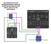
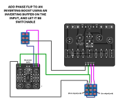
Hi again.. Now that I've been placed on the right track by you guys, is this the way i would want to wire it to have the inverter board be a flippable input stage for the main circuit, and have the pedal remain as true bypass?
NON-NVERTED- Fumble Boost - PedalPCB.com v2.png
 
Last edited:
You don't need a DPDT, a SPDT would work, then wire the input jack side of the 3DPT just straight to the input of the inverter PCB.

The way you have it wired wouldn't hurt anything though, just isn't totally necessary and will save some space in the box to use a SPDT.
 
You don't need a DPDT, a SPDT would work, then wire the input jack side of the 3DPT just straight to the input of the inverter PCB.

The way you have it wired wouldn't hurt anything though, just isn't totally necessary and will save some space in the box to use a SPDT.
thank you. i already have a bunch of the mini dpdt's from projects unrelated to pedals.. i'm still going to do what you're saying though, because less wire
 
thank you. i already have a bunch of the mini dpdt's from projects unrelated to pedals.. i'm still going to do what you're saying though, because less wire
Sounds good! If you don't have any SPDT just use what you have of course!

I did this awhile back (mostly talking to myself but got some good advice) https://forum.pedalpcb.com/threads/phase-inverting-at-input-buffer-vs-after-effect.24318/

The PPCB board didn't exist yet at that time, if it had I probably would have snagged one instead (along with a microblend board) of stumbling through it myself. I was able to get it working without a board spin though so all good!

Also, here is the schematic of the board if you don't already have it:

 
Also no need to edit your original post! I think keeping the questions as-is, keeps the answers making sense and then someone else who maybe has the same question can learn the same way!
 
Also no need to edit your original post! I think keeping the questions as-is, keeps the answers making sense and then someone else who maybe has the same question can learn the same way!
true.. that's why i'd struck the mistaken premise out instead of deleting it. I can put it back though..
here's an updated image for anyone who lands here. thanks again!
 

Attachments

  • NON-NVERTED- Fumble Boost - PedalPCB.com v2-fixed.png
    NON-NVERTED- Fumble Boost - PedalPCB.com v2-fixed.png
    216.6 KB · Views: 2
Last edited:
Back
Top