It's a network flag, as are VCC, VDD, VRef, etc. It's basically a shorthand way of saying "connect all of these points" without having to draw a bunch of connection wires, which makes for a schematic that's easier to read.
It's a network flag, as are VCC, VDD, VRef, etc. It's basically a shorthand way of saying "connect all of these points" without having to draw a bunch of connection wires, which makes for a schematic that's easier to read.
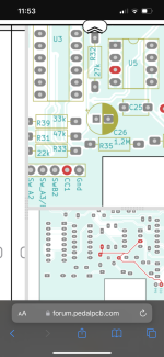
This seems to differ from other electric mistress schematics I’ve seen. That node is connected to the clock input of the CD4013. It may just be a test point for the VCO trim. Not entirely sure why that’s being brought out with the other supply pins. Do you have any other documentation? Is there a daughterboard?
This seems to differ from other electric mistress schematics I’ve seen. That node is connected to the clock input of the CD4013. It may just be a test point for the VCO trim. Not entirely sure why that’s being brought out with the other supply pins. Do you have any other documentation? Is there a daughterboard?
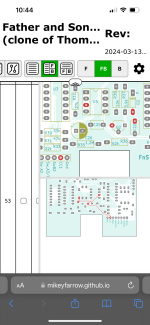
The documentation I have is on this Github repository. I don't really know what any of this stuff is. I asked my brother to find me an electric mistress clone, and he found this one and then had the circuit boards fabricated.