What is the ring around the power section on the Skeptical Buffer PCB?

Many__Of__Horror

Active member
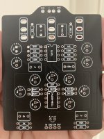
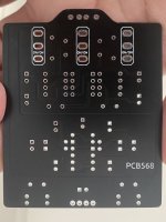
I saw someone post an image of the Skeptical Buffer PCB on the forum & I was curious on what the surrounding area around the power section on the front and back of the PCB was called and it's benefits. I assume isolation? The back area goes to the power input but the front is just around the power section.
 

Attachments

  • IMG_8372.jpeg
    IMG_8372.jpeg
    425.5 KB · Views: 56
  • IMG_8371.jpeg
    IMG_8371.jpeg
    364.4 KB · Views: 55
Those lines are the copper traces that route power and signals around the PCB. They are important because they distribute the power and signal around the board to the various components.
 
Back
Top