You are using an out of date browser. It may not display this or other websites correctly.
You should upgrade or use an alternative browser.
You should upgrade or use an alternative browser.
Getting Started with PCBA at JLCPCB
- Thread starter z2amiller
- Start date
- Featured
z2amiller
Member
Yep - I listed it in my guide, it's the Bouni plugin for Kicad. It lets you do the parts assignment as a separate step.KiCAD has a specific plugin I believe.
Rpschultz13
Well-known member
Great thread. The EOL date for Eagle has been looming, and I have wanted to learn SMDA so I took the plunge into EasyEDA. 2 weeks in, I've got most of it figured out.
For Q-tune, I've been able to take the thru-hole design in Eagle, and (starting from scratch), re-create an SMDA version in EasyEDA. It took some learning, but EasyEDA is absolutely easy. I highly recommend it, integration with JLC is cake.
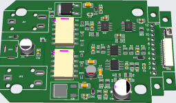
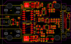
See Q-tune 4-layer SMD version, I got everything SMDA except the 3 jacks on the left. For example, the thru-hole PCB's cost about $1, and SMDA will cost about $7 each. But I'll save more than that on the components, so it's a win. AND 90% of it is assembled.


Based on the info in post #1, I need to look into a few things:
For Q-tune, I've been able to take the thru-hole design in Eagle, and (starting from scratch), re-create an SMDA version in EasyEDA. It took some learning, but EasyEDA is absolutely easy. I highly recommend it, integration with JLC is cake.
See Q-tune 4-layer SMD version, I got everything SMDA except the 3 jacks on the left. For example, the thru-hole PCB's cost about $1, and SMDA will cost about $7 each. But I'll save more than that on the components, so it's a win. AND 90% of it is assembled.


Based on the info in post #1, I need to look into a few things:
- 0603 resistors instead of 0805
- SOP-8 instead of SOIC-8 for op amps (SOP-8 is a little bigger though)
- Review all my cap selections. I found a 100n C0G/NP0 (1206) for audio. But I need to check the rest.
z2amiller
Member
Looks awesome! Stick with the SOIC-8's vs SOP-8's, I misspoke in the original post - it's all SOIC-8 that are the 'basic' op-amps.
For the Q-Tune I imagine you're probably assembling enough of these ( >= 50 ) that you're into 'Standard' assembly
anyway so you don't need to worry as much about price hacking the basic components? Aside from prototyping/test
runs of course.
I noticed a lot of your pads are quite a lot larger than necessary (IC1 in particular looks like it might even be
the wrong footprint) - are you using handsoldering pad shapes?
Personally I try to use bigger traces on my layouts - I can't remember what the default is in EasyEDA but in Kicad it's a teeny tiny
0.2mm. I try to use 0.5mm even for signals which means no routing underneath most passives, but I try not to do that anyway.
I did some initial designs in EasyEDA but ended up porting to KiCAD - mostly to get source control plugins, and feeling
less locked-in to a particular ecosystem.
I do miss the web-based nature of EasyEDA though, since it's all web based it's nice to be able to work on my desktop and
then pick up right where I left off on my laptop. (Which of course I can do with the source control plugins but that's not as convenient).
It's also pretty amazing how well integrated things are with LCSC parts - the footprints and order numbers and everything
is right in there and searchable so it's super easy to go from design to production.
Rpschultz13
Well-known member
Op amp wise, the only Basic I found was the TL072. I can't find a basic one for MCP6002, and more strangely, I can't find a basic NE555 timer?!? Oh well. But yes you're right, SOIC-8 is generally best. I'm using the standard footprints that come in EasyEDA. The only footprint I created was for the audio jacks.
I'm not sure if by Standard, you mean in JLC Standard vs Economic?!? Initially I tried assembly on both Top and Bottom, but that tripped it over to Standard and the cost went up a LOT. So I'm sticking with assembly on just the Top.
Yes on the traces, I need to fix many of them. EasyEDA defaults to 1/4mm. I need to do some research on what is best. I'll probably ask the guys on AAC for advice on that. Sigal traces are low current/power. But power traces are more so definitely want those to be wider.
We used Kicad to augment Eagle with the thru-hole board for Q-tune, Kicad gives WAY better flexibility with footprints. But after using EasyEDA for 2 weeks, it's light years ahead of both. Makes Eagle feel like a dinosaur. It's so integrated with JLC/LCSC, really nice. You should give it a 2nd look. The autorouter also works pretty well too. With a 4 layer I tend to manually route most anyway, but the AR works.
I switched all my resistors over to 0603, nice tip!
z2amiller
Member
Op amp wise, the only Basic I found was the TL072.
I haven't used the search tool within EasyEDA, but using their parametric search:
(https://jlcpcb.com/parts/all-electronic-components - and checking the 'basic' and 'promotional extended' boxes)
C6961: TL072CDT
C7426: NE5532DR
C7433: OP07CDR
C7950: LM358DR2G
C18229: LM2904DR2G
(and a couple more)
and notably, in the 'Promotional Extended' parts which you don't pay setup for:
C7377: MCP6002T-I/SN
and
C7593: NE555DR
I'm not sure if by Standard, you mean in JLC Standard vs Economic
Yeah - both sides will tip you to standard, and going over 30-50 pieces (depending on ... something I'm not sure of) will also put you into Standard.
Rpschultz13
Well-known member
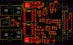
I did some digging on trace width. For signals, the default of 0.254mm (0.1") is completely adequate. Even for power that's probably fine. I did some calcs with 150 mA of current on an internal layer (hotter), and it only requires a trace width of 0.05 mm. 150 mA is a lot of current for most pedals - it is the current draw of the esp32 screen we use on Q-tune. Now practically if space allows, making the power traces wider can't hurt. On a 4-layer board where an inner layer is only for power, there's plenty of room.
Below picture, power in green, signal red/blue:
a) kept the signal traces at 1/4mm
b) widened primary power leads to 3/4mm
c) widened the secondary power (after regulators, etc) to 1/2mm
d) notice the added vias on the ground in the regulators. I've been told, more vias the better, pretty much everywhere.
I think the above is completely overkill, but so easy, why not.

vigilante398
Authorized Vendor
They actually used to have a basic NE555, that went away a while ago. Apparently the basic component list changes based on what they feel like carrying. I've had to change a couple of the resistors I use based on basic part changes over the years as well.I can't find a basic NE555 timer?!?
Great thread. The EOL date for Eagle has been looming, and I have wanted to learn SMDA so I took the plunge into EasyEDA. 2 weeks in, I've got most of it figured out.
For Q-tune, I've been able to take the thru-hole design in Eagle, and (starting from scratch), re-create an SMDA version in EasyEDA. It took some learning, but EasyEDA is absolutely easy. I highly recommend it, integration with JLC is cake.
See Q-tune 4-layer SMD version, I got everything SMDA except the 3 jacks on the left. For example, the thru-hole PCB's cost about $1, and SMDA will cost about $7 each. But I'll save more than that on the components, so it's a win. AND 90% of it is assembled.
View attachment 103068
View attachment 103069
Based on the info in post #1, I need to look into a few things:
- 0603 resistors instead of 0805
- SOP-8 instead of SOIC-8 for op amps (SOP-8 is a little bigger though)
- Review all my cap selections. I found a 100n C0G/NP0 (1206) for audio. But I need to check the rest.
So the electro caps didn't bump you over to standard?
Rpschultz13
Well-known member
No the 3 electrolytics are extended but still economic not standard. The only thing that tripped me over to standard was assembly on both sides. Initially I wanted the 12-pin JST on the bottom, but it increased the cost a lot. So I found a way to put it on top and keep it economic top side assembly only.So the electro caps didn't bump you over to standard?
Last edited:
Rpschultz13
Well-known member
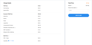
Here was my latest cost for 5 assembled prototypes, just to give an idea on cost. $30 extended fee means I had 10 extended components $3 each. But everything else is so cheap, all the resistors and most of the caps/diodes are basic, literally pennys. They also allow an initial 5 boards but only assemble 2. I could do that for $75 shipped. Seems reasonable for prototyping.


vigilante398
Authorized Vendor
I've seen inconsistency there. Most of my stuff is standard anyway, but every now and then I have a design I think can be economic and the electros bump it to standard, where other times they don't. Not sure what the actual rule is.So the electro caps didn't bump you over to standard?
z2amiller
Member
I've seen inconsistency there. Most of my stuff is standard anyway, but every now and then I have a design I think can be economic and the electros bump it to standard, where other times they don't. Not sure what the actual rule is.
Yeah - I mentioned this in my guide - when you're looking for components you can filter on 'Economic'. I've also noticed that
with electrolytics, there are some of them that will bump your board to standard assembly. I'm not 100% sure what the reason
is, but I suspect that it has something to do with the reels or the shape of the components that don't work well in the standard
pick and place machines, or have more stringent temperature requirements or something. I notice this especially with the
'ROQANG' brand electrolytics which are also the ones that JLC has a ton of and sorts to the top of the list as the cheapest
How about clearance specs? I’ve been using .254” as well for signal and just used the same spec for minimum clearance but i wonder if it can safely go tighter?I did some digging on trace width. For signals, the default of 0.254mm (0.1") is completely adequate. Even for power that's probably fine. I did some calcs with 150 mA of current on an internal layer (hotter), and it only requires a trace width of 0.05 mm. 150 mA is a lot of current for most pedals - it is the current draw of the esp32 screen we use on Q-tune. Now practically if space allows, making the power traces wider can't hurt. On a 4-layer board where an inner layer is only for power, there's plenty of room.
Below picture, power in green, signal red/blue:
a) kept the signal traces at 1/4mm
b) widened primary power leads to 3/4mm
c) widened the secondary power (after regulators, etc) to 1/2mm
d) notice the added vias on the ground in the regulators. I've been told, more vias the better, pretty much everywhere.
I think the above is completely overkill, but so easy, why not.
View attachment 103084
I know i said it once already but this is a GREAT freaking thread
Asdrael
Well-known member
Creepage depends on what the trace is carrying. You have creepage required for safety against arcing (purely voltage related and below 9V you can go really tight) but then there is creepage that is specific to coupling between signal. Then you should take into a count not only the voltage difference but impedance. And also looping issues when you have one trace and “it’s ground return” too close.
I am more into amps when it comes to guideline for this but: know what each trace actually is, have a set of conservative rules for general tracing and don’t be scared of using necks here and there for safety. Better a neck than an arc or coupling!
I am more into amps when it comes to guideline for this but: know what each trace actually is, have a set of conservative rules for general tracing and don’t be scared of using necks here and there for safety. Better a neck than an arc or coupling!
I assume this logic applies to clearance between traces/pads and the ground pour as well? I try to keep traces and pads well away from each other when possible… SMT is a very different animal from laying out a through hole board in that regard for sure though.Creepage depends on what the trace is carrying. You have creepage required for safety against arcing (purely voltage related and below 9V you can go really tight) but then there is creepage that is specific to coupling between signal. Then you should take into a count not only the voltage difference but impedance. And also looping issues when you have one trace and “it’s ground return” too close.
I am more into amps when it comes to guideline for this but: know what each trace actually is, have a set of conservative rules for general tracing and don’t be scared of using necks here and there for safety. Better a neck than an arc or coupling!
Rpschultz13
Well-known member
Please elaborateYes same for ground pours. And keep in mind good grounding practice - not all grounds traces are equal, even if they end up tied at the same spot.
Rpschultz13
Well-known member
Regarding grounds. I’m no expert. But I’ve been told that a 4 layer board with an inner ground layer and the other 3 with ground planes is FAR superior to a 2 layer board with ground planes.
I’ve recently learned how to do this in EasyEDA, it’s practically the same price as a 2 layer at JLC.
I’ve recently learned how to do this in EasyEDA, it’s practically the same price as a 2 layer at JLC.
