You are using an out of date browser. It may not display this or other websites correctly.
You should upgrade or use an alternative browser.
You should upgrade or use an alternative browser.
Bring out yer Diptrace
- Thread starter Grubb
- Start date
iamjackslackof
Well-known member
Is this going to end up on your Github? And is the SOIC8 part a microcontroller?Another SMD prototype, now the basic relay:
View attachment 53184
finebyfine
Well-known member
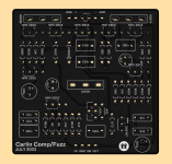
Haven't sent any off in a few weeks, just ordered this board for the Carlin Compressor / Fuzz. Frustrating as all hell to lay out with any semblance of order especially with the cockamamie expanded pinout transistor footprint. Working on one for Carlin's Ring mod now


iamjackslackof
Well-known member
Adding the pinout is an amazing addition! I wish it was standard.
finebyfine
Well-known member
Adding the pinout is an amazing addition! I wish it was standard.
It’s SO helpful when building but it can be such an annoying hurdle for laying out traces to have to make that many extra connections. I rarely do it but need to stick to them
szukalski
Well-known member
This is Chucks basic relay design, the IC is just a 555. I need to do some testing before I think about open sourcing it. The through hole version is ready for the GitHub though, I just need to get around to it.Is this going to end up on your Github? And is the SOIC8 part a microcontroller?
The through hole version is small enough to retrofit to any build (and using pin headers which makes building even easier).
finebyfine
Well-known member
@szukalski do you use diptrace for designs to send off for jlcpcb’s smd assembly service? I’ve only used EasyEDA when doing that and was wondering if if you do use Diptrace if you have any tips beyond jlcpcb’s instructions. TIA!
szukalski
Well-known member
I've just done my first, so I'll tell you once I get them back.@szukalski do you use diptrace for designs to send off for jlcpcb’s smd assembly service? I’ve only used EasyEDA when doing that and was wondering if if you do use Diptrace if you have any tips beyond jlcpcb’s instructions. TIA!
The main thing is setting up the Diptrace library, that's time consuming. I'm slowly building mine up (and sharing the sheepy love):
sheepylove-diptrace/Sheepylove_JLC at main · szukalski/sheepylove-diptrace
Diptrace library for building PCBs. Contribute to szukalski/sheepylove-diptrace development by creating an account on GitHub.
I just followed JLC's instructions, but noticed that they had to change the offset of components for me, which is fine if they do it each time, but it'd be good to know how to do it correctly.
vigilante398
Authorized Vendor
Yup, should be possible in Diptrace. This is common in mixed-signal design, using separate ground pours for digital and power ground, digital and analog ground, high-speed/RF and low-speed ground, etc., then connecting the two either with a single 0Ω resistor or with a net tie.Possible stupid question that I can’t answer for myself right now because I’m away from Diptrace:
Can you create multiple “ground islands” for lack of a better term in Diptrace? Kind of like individual ground planes for circuit chunks on a single side?
I’m investigating isolating the grounds a few circuit chunks and bringing the, together with jumper resistors right at the DC connection.
Harry Klippton
Not Interested
are y'all using a different hole size for pads that will get pin headers? Tayda's datasheet says the pins on their headers are .64mm in diameter, and Diptrace's standard pad hole size is .7mm. what say you? paging @szukalski
vigilante398
Authorized Vendor
I usually use 40mil (~1mm) holes for through-hole things, which is a luxurious fit for headers. On more compact things where space is a premium I'll go down to 35mil (~0.889mm) which is a little more snug. Don't think I've ever gone smaller than that personally.are y'all using a different hole size for pads that will get pin headers? Tayda's datasheet says the pins on their headers are .64mm in diameter, and Diptrace's standard pad hole size is .7mm. what say you? paging @szukalski
JamieJ
Well-known member
What size traces do you use with tube circuits @vigilante398
Also what do you do interns of space between ground and traces?
Also what do you do interns of space between ground and traces?
szukalski
Well-known member
My standard pad hole is 0.9mm, with the pad being 1.5mm. I don't differentiate between pins or other pads (except pots and switches).are y'all using a different hole size for pads that will get pin headers? Tayda's datasheet says the pins on their headers are .64mm in diameter, and Diptrace's standard pad hole size is .7mm. what say you? paging @szukalski
For pots, it's 1.4mm and 2.54mm respectively.
Trace width and clearance is 0.254mm, more if I work with HV but there are other who have that well in hand so I haven't done much
Harry Klippton
Not Interested
Thanks y'all
szukalski
Well-known member
Loving it. I would also recommend making a jig so you can solder the DC jack in the right place. I usually use a bit of blu-tack and align up with the enclosure holes, but it's annoying and not scalable. You could easily make a PCB jig/frame.Threw this together this morning, inspired by comments from @szukalski:
vigilante398
Authorized Vendor
I typically do 15mil signal traces and keep them as far apart as possible. Most of my boards these days are 4-layer, so I have a dedicated ground place and a split power plane. When routing gets tight I allow DC lines (ground, power) to be closer to audio signals, but I try to keep audio signals as far apart from each other as possible.What size traces do you use with tube circuits @vigilante398
Also what do you do interns of space between ground and traces?


