You are using an out of date browser. It may not display this or other websites correctly.
You should upgrade or use an alternative browser.
You should upgrade or use an alternative browser.
Bring out yer Diptrace
- Thread starter Grubb
- Start date
Smrtokvitek
Well-known member
finebyfine
Well-known member
What is your recommended pcb width for the 125B enclosure? @PedalPCB boards are usually 1.9in, but I feel a 2.3in should be doable.
I think the Tayda 125B has supposedly changed recently but I've gotten as wide as 60.96mm (2.4in) before although it's definitely close as hell to the edges - I gotta imagine I stole that from Rob somewhere.
I tried to confirm I stole that from Rob and looked up some of the wider boards for what its worth:
- 2.35in (59.69mm) wide: Ocelot, Parenthesis Mini, Abider, Dirty Sanchez, Derailer, Mofeta, Polonium, SMD Scream Machine, Wilhelm Scream
- 2.375in (60.325mm) wide: FV1 Dev Board, Wrectifier
Last edited:
vigilante398
Authorized Vendor
I do 2.1" for my 125B designs and it's got wiggle room so I know you can go bigger, but I'm too lazy to change my template.
neiltheseal
Well-known member
This looks great. Do you have a schematic for the relay switch that you used?Another revision based on dry fitting and real wiring of the test units:
View attachment 52197
1.) I made the board 1mm narrower overall
2.) I had to switch to a shallower Eagle Plastics ground spring because the Keystone was bottoming out
3.) Switched to the 8 Pin Fujitsu relay based on @szukalski advice
4.) Spaced things out a little more, as I found some of the stuff was a bit tight
Robert
Reverse Engineer
You can go as wide as 59mm in my experience. That’s the standard width of my 125B boards.
My standard is 2.35" width for 125B.
The FV-1 Dev board is 2.375" wide so the PCB is flush against the enclosure on both sides to accommodate the USB port (and prevent the board
from shifting from side to side when plugging the cable in).
neiltheseal
Well-known member
Will this work?The relay is a Fujitsu FTR-B3CA4.5Z
Datasheet:
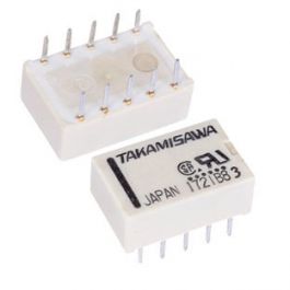
Mini Relay DPDT A-4.5W-K 4.5VDC 10PIN 2Poles 1A
FUJITSU COMPONENTS - Get It Fast - Same Day Shipping
 www.taydaelectronics.com
neiltheseal
Well-known member
Thanks. I'd ideally like to make my own for the circuits I'm sending to JLPCB.I buy lots of stuff from Tayda so that's easy. I there a good resource for relays? Istruggle to read the datasheets for them. They are not what I'm used to such as ICs and transistors.Yeah. It’s the same relay just the End of Life 10 pin version.
@szukalski hipped me to the one I sent you because it’s a current model (no new design concerns with being obsolete) and it’s cheaper.
If you are using a Pedal PCB relay bypass, you’ll want the 10 pin though.
szukalski
Well-known member
Thanks. I'd ideally like to make my own for the circuits I'm sending to JLPCB.I buy lots of stuff from Tayda so that's easy. I there a good resource for relays? Istruggle to read the datasheets for them. They are not what I'm used to such as ICs and transistors.
There are tons of cross reference sheets out there for various manufacturers (tyco, omron, Fujitsu)Thanks. I'd ideally like to make my own for the circuits I'm sending to JLPCB.I buy lots of stuff from Tayda so that's easy. I there a good resource for relays? Istruggle to read the datasheets for them. They are not what I'm used to such as ICs and transistors.
If you know one model that works, you can reference them to find alternatives easy.
Omron Cross Reference https://www.casa.co.nz/electrics/relays/RELAYS-CROSS-REF.pdf
neiltheseal
Well-known member
Thanks so much. This is really helpfulLet's do an example using the Pedal PCB Basic Relay Bypass as reference and the A-4.5W-K:
View attachment 56910View attachment 56909
The A-4.5W-K is a non-latching relay, meaning it is NC without power and NO when power is applied and energizing the coil, shown as Pins 1 and 10.
The datasheet shows the de-energized condition, meaning that without power, the relay will put the pedal in true bypass condition. The de-energized state is shown in the Pedal PCB schematic, with Pins 2 and 9 active on the relay.
When power is applied, the relay changes state to pins 4 and 7.
It's important to remember that Pins 2, 3, 4, 7, 8, and 9 form a 3PDT switch, just like any other bypass switch. Pins 1 and 10 are the energization/closing/actuation coil, meaning that depending on the type of relay, energization vs. de-energization of the coil operates the switch contacts.
As far as implementing relays into PCB footprints or existing layouts, it is important to keep two things in mind:
1.) The orientation mark denotes the energization coil end
2.) The footprints on the datasheets are BOTTOM views typically.
With respect to 2.) it is important to orient your PCB footprint properly:
View attachment 56911 View attachment 56913
finebyfine
Well-known member
whewiee


finebyfine
Well-known member


benny_profane
Well-known member
Option for integrated relay switching?It always feels like a waste to have a chunk of PCB unused
szukalski
Well-known member
I like to keep it off-board. The relay solutions I have are small enough, and I like to give other builders the option to choose their path.Option for integrated relay switching?
I am thinking of an on-board set boost with a toggle switch though. The circuit is mid-high gain and really takes off with a boost (though so does the noise).
Harry Klippton
Not Interested
What if you incorporated it with the option to jumper it in, or leave it unattached?I like to keep it off-board. The relay solutions I have are small enough, and I like to give other builders the option to choose their path.
I am thinking of an on-board set boost with a toggle switch though. The circuit is mid-high gain and really takes off with a boost (though so does the noise).