Looking for some MN3101 clone beta testers (CT3101)

Cabintech

Authorized Vendor
Hi all, we have developed a simple drop-in replacement for the MN3101 BBD clock chip for use with MN300X series BBDs. The CT3101 is a small PCB with the same DIL-8 footprint and same pinout as the MN3101. It is based on the CD4047 and includes the Vgg (14/15 Vdd) output voltage, and supports supply voltages to -18V.

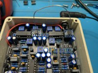
It has been bench-tested and verified in a few products (including the MOE AC60, photo below, and Juno 106) but we are seeking beta testers who would be willing to try these in a wide variety of devices to make sure they work in various operating conditions and circuit designs. Ideally, when swapped with an MN3101 there would be no discernable difference in sound or function.

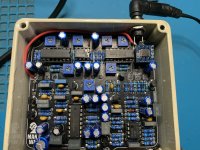
Here is a photo of the CT3101 modules in sockets along side two MN3009s in the AC60:
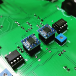
1691351940295.png

If you are interested in giving these a try, we will send you 2 prototype samples at no cost. We only ask that you try them in devices that currently use MN3101 chips and report back to us what device you put them in, and how they worked or any problems you noticed. (If you need more than 2 let us know, we have a limited prototype supply). You are welcome to post your results here or (if your design is confidential) by email or PM. We would be particularly interested in flangers (see design notes below).

Send us a PM with your shipping address and what device(s) you will be testing and we will ship them to you in the next few days.

Thanks!
Mark McMillan
Cabintech Global LLC

Background:
For years customers have been asking us to sell MN3101 chips or help them find a reliable supply. As a policy, we prefer not to deal in so-called "New Old Stock" (NOS) devices (although we did for a while during the pandemic/chip shortage). Always we told them, the MN3101 is long out of production and there is no current clone manufacturer... we don't carry the MN3101 and good luck finding ones that are not fake or have high fall-out rates. You might get lucky on Ebay and find one that works. A number of alternatives are available to produce the required BBD 2-phase clocks, but that does not help someone trying to repair an existing device or build a kit designed for the 3101.

It did not seem so hard to make a clone, the concepts of a multivibrator circuit are well understood. So finally we started down the path of a new chip design (it is not particularly difficult), but then the chip shortage hit and we had to abandon that idea. Also the quantities needed to make them cost effective were quite high. So instead we considered a hybrid module (PCB with a DIL-8 footprint and pinout identical to the MN3101). These are easy to manufacturer in reasonable quantities and allow us to use inexpensive off-the-shelf parts instead of a custom chip design. This idea sat on the shelf for a while until Made On Earth needed some BBD chips and mentioned they were having trouble sourcing the 3101s needed to make them work. So we collaborated with them on a design for the CT3101 and we recently verified it in their AC60 analog chorus pedal design. It has also been verified in the Juno 106 (and presumably, the similar Juno 6 and 60).

The Design:
The CT3101 design is quite simple, it is a CD4047 with a decoupling cap and a voltage divider network (to generate Vgg output). Because the CD4047 is a +V device, ground and power on the PCB are reversed relative to the MN3101 Vdd/GND pins. The PCB contains the interconnect to configure the CD4047 and route inputs and outputs to the MN3101 pinout. The 8 DIL pins are not common header pins that are often too big to fit into DIP sockets, but smaller round pins that allow the module to be socketed easily or soldered in through-hole designs. The PCB is slightly larger than an actual MN3101 DIL package so it may be a tight mechanical fit in very crowded system designs if other components are very close to the MN3101.

There is no output driver, so output current is limited to what the CD4047 can source. This may prove problematic at high frequencies, we don't know yet if it is a practical issue in real high frequency designs (e.g. flangers).
 
First off, I want to say thanks to Mark and the good folks at @Cabintech for sending me the chips and allowing me to participate in this testing.

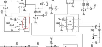
I tested two of these CT3101s in a Madbean Man O’ War delay. It’s modeled after the Maxon AD-900, runs at 12 volts, and utilizes a main and slave MN3101 to drive the BBDs. That being said, I found a problem right away with my initial bench test. The circuit does not work properly with two CT3101s for both clock chips. There was no clock signal coming out of pins 2 and 4 of either clock driver in this configuration. After some more debugging, I discovered the CT3101 will not work in the IC4 position specifically but, works just fine in IC6 as long as a genuine MN3101 is in IC4. On the schematic, I noticed that pins 5 and 7 aren’t connected to anything so I believe this is why the CT3101 doesn’t work in position IC4 but works in IC6.
IMG_2260.jpeg

With a CT3101 in IC6 and a MN3101 in IC4, there’s a good clock signal coming out of pins 2 and 4 of both chips and the delay works like normal.

IMG_2258.jpeg

With the CT and MN combo, I maxed the delay knob and dialed in a clock frequency of 7khz. Setting the delay knob to minimum equated to a clock speed of 117khz which is exactly what I was getting previously with two MN3101s in place.

With this combo of clock chips I also did a sound test on my main guitar rig. I observed no abnormal sounds or behaviors. I tried several different modulation pedals in front of and behind the delay and there were no weird interactions. The delay sounded exactly how it’s always sounded. The CT3101 seems to work as a MN3101, as long as all the pins are utilized.
 
Last edited:
The circuit does not work properly with two CT3101s for both clock chips. There was no clock signal coming out of pins 2 and 4 of either clock driver in this configuration. After some more debugging, I discovered the CT3101 will not work in the IC4 position specifically but, works just fine in IC6 as long as a genuine MN3101 is in IC4. On the schematic, I noticed that pins 5 and 7 aren’t connected to anything so I believe this is why the CT3101 doesn’t work in position IC4 but works in IC6....

Wow, thanks for the excellent testing and debugging!

That circuit design is interesting. It seems that both clock chips will put out the same frequency -- IC4 does not oscillate, but is driven by the oscillation of IC5 so both clocks run at the same speed. So I wonder why there are two clock chips at all, the MN3101 is spec'ed to drive (2) MN3005s, so why use two chips to drive 2 MN3005s? Unless these are run at very high frequency (e.g. 1MHz range) using 2 clock drivers seems unnecessary (and even then, a line driver would be a simpler solution for driving more current than using two clock chips).

But OK, given 2 linked clock chips, the linking seems wrong. Pin 6 of IC5 outputs the oscillation frequency, but pin 6 of IC4 is normally an output -- driven by an inverter from pin 7. But it is being driven as an input. The MN3101 datasheet indicates that for external excitation, "OX3 (pin 5) and OX2 (pin 6) are open and OX1 (pin 7) is the oscillation input". If pin 7 is floating, then pin 6 is being driven internally to some indeterminate state. Seems like that would be fighting the use of pin 6 as an input.

Can you trace the PCB and verify that pin 6 of IC5 is going to pin 6 of IC4, and that pins 5 and 7 of IC4 are really N.C.? I am hoping the schematic is wrong because it makes no sense to me!

Thanks!
-Mark
 
I've been wondering when someone would look into making new MN3101 clocks for a while now (as @StompBoxParts can attest to). I'm glad you are working on a solution to this issue! I've even been shying away from developing projects that use that clock due to the lack of legit availability of 3101's.
 
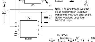
PS. A quick google for AD-900 schematics turned up this one which someone manually traced the circuit to produce, and it shows the slave MN3101 is driven from pin 7, not pin 6. This is what I would expect. And I think I know why the CT1301 does not operate correctly in this configuration.


1691681665532.png
 
Wow, thanks for the excellent testing and debugging!

That circuit design is interesting. It seems that both clock chips will put out the same frequency -- IC4 does not oscillate, but is driven by the oscillation of IC5 so both clocks run at the same speed. So I wonder why there are two clock chips at all, the MN3101 is spec'ed to drive (2) MN3005s, so why use two chips to drive 2 MN3005s? Unless these are run at very high frequency (e.g. 1MHz range) using 2 clock drivers seems unnecessary (and even then, a line driver would be a simpler solution for driving more current than using two clock chips).

But OK, given 2 linked clock chips, the linking seems wrong. Pin 6 of IC5 outputs the oscillation frequency, but pin 6 of IC4 is normally an output -- driven by an inverter from pin 7. But it is being driven as an input. The MN3101 datasheet indicates that for external excitation, "OX3 (pin 5) and OX2 (pin 6) are open and OX1 (pin 7) is the oscillation input". If pin 7 is floating, then pin 6 is being driven internally to some indeterminate state. Seems like that would be fighting the use of pin 6 as an input.

Can you trace the PCB and verify that pin 6 of IC5 is going to pin 6 of IC4, and that pins 5 and 7 of IC4 are really N.C.? I am hoping the schematic is wrong because it makes no sense to me!

Thanks!
-Mark
Here’s the link to Brian’s build docs for this circuit. https://www.madbeanpedals.com/projects/_folders/Delay/pdf/ManOWar.pdf

If you look at the trace diagram, pin 6 of IC5 goes to pin 4 of IC6. Pin 4 of IC4 is connected to pin 6 of IC3 and pin 6 on both clock chips is indeed connected. I can trace the pcb later today to confirm. Hopefully I’m not out of line here by bringing Brian into this but, maybe @bean can chime in with a quicker answer.
 
Wow, thanks for the excellent testing and debugging!

That circuit design is interesting. It seems that both clock chips will put out the same frequency -- IC4 does not oscillate, but is driven by the oscillation of IC5 so both clocks run at the same speed. So I wonder why there are two clock chips at all, the MN3101 is spec'ed to drive (2) MN3005s, so why use two chips to drive 2 MN3005s? Unless these are run at very high frequency (e.g. 1MHz range) using 2 clock drivers seems unnecessary (and even then, a line driver would be a simpler solution for driving more current than using two clock chips).

But OK, given 2 linked clock chips, the linking seems wrong. Pin 6 of IC5 outputs the oscillation frequency, but pin 6 of IC4 is normally an output -- driven by an inverter from pin 7. But it is being driven as an input. The MN3101 datasheet indicates that for external excitation, "OX3 (pin 5) and OX2 (pin 6) are open and OX1 (pin 7) is the oscillation input". If pin 7 is floating, then pin 6 is being driven internally to some indeterminate state. Seems like that would be fighting the use of pin 6 as an input.

Can you trace the PCB and verify that pin 6 of IC5 is going to pin 6 of IC4, and that pins 5 and 7 of IC4 are really N.C.? I am hoping the schematic is wrong because it makes no sense to me!

Thanks!
-Mark
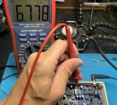
So, I traced out the pcb and did a continuity check with a multimeter. I can confirm that pin 6 of IC4 and IC6 are connected.
 
Here’s the link to Brian’s build docs for this circuit. https://www.madbeanpedals.com/projects/_folders/Delay/pdf/ManOWar.pdf

If you look at the trace diagram, pin 6 of IC5 goes to pin 4 of IC6. Pin 4 of IC4 is connected to pin 6 of IC3 and pin 6 on both clock chips is indeed connected. I can trace the pcb later today to confirm. Hopefully I’m not out of line here by bringing Brian into this but, maybe @bean can chime in with a quicker answer.


Well, I'll be doggone. That is definitely a damn mistake on my part. It should be connected to the input OSC pin and it's connected to the output. This was the only delay circuit I had worked on that used a slaved clock so my inexperience at that point is to blame. But, I do remember getting the correct delay amount out of the two BBDs so it does partially work somehow.

In any case, it's wrong. I'll come up with a workaround and update the doc, and post a thread on the mbp forum. Thanks for bringing this to my attention.

Both the MN3101 and CD4047 are CMOS devices which in general have rather undefined behavior with unconnected gate inputs.
There must be some detail of the MN3101 output gate circuit that allows it to be driven backwards from the output pin and thus drive the next inverter inside the chip. Apparently it works well enough with the MN3101 that it never caused a problem in this design.

I would still like to verify the CT3101 works if the circuit is corrected to drive IC4 on pin 7 and leave pin 6 unconnected.
 
So, I traced out the pcb and did a continuity check with a multimeter. I can confirm that pin 6 of IC4 and IC6 are connected.
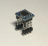
It would be great if we could swap pins 6 and7 on IC4 to verify the CT3101 works properly there. I cannot think of a way to do that on the PCB without destructive PCB changes (e.g. cut traces). If you are game and handy with a soldering iron, you could build an adapter from 2 bits of header strip. We did something similar with an early prototype -- this one swaps pins 5 and 6. You could cut off the CT3101 pin 6 (or just bend it out of the way), then cross over header pin 6 to leg 7 of the CT3101.

1691763289388.png

We can make up something like that for you and send it in the mail to try if you want (I know you already put plenty of time into this...)

Thanks!
-Mark
 
It would be great if we could swap pins 6 and7 on IC4 to verify the CT3101 works properly there. I cannot think of a way to do that on the PCB without destructive PCB changes (e.g. cut traces). If you are game and handy with a soldering iron, you could build an adapter from 2 bits of header strip. We did something similar with an early prototype -- this one swaps pins 5 and 6. You could cut off the CT3101 pin 6 (or just bend it out of the way), then cross over header pin 6 to leg 7 of the CT3101.

View attachment 54385

We can make up something like that for you and send it in the mail to try if you want (I know you already put plenty of time into this...)

Thanks!
-Mark
I was already planning on messing with it this weekend so it’s all good and I’m happy to help. I’ll be sure to post my test results.
 
Good news! I lopped off pin 6 on the ct3101 in IC4, tack soldered some bus wire from IC6 pin 6 to pin 7 of IC4… and she’s working. Did a quick test with my guitar through the bench amp and I have a working delay with two CT3101s in place.
That is awesome! Thanks for all the great debugging work!

Whew. Glad that is sorted, was a bit worried by this one since we did not explicitly test that configuration. I guess that's what 'beta' is for :).
 
One question I thought of - if you were to make the VGG voltage divider empty through-hole (say 1/8W) instead of pre-populated SMD resistors then would the builder be able to tailor the CT3101 to drive MN320x chips, as well?
 
One question I thought of - if you were to make the VGG voltage divider empty through-hole (say 1/8W) instead of pre-populated SMD resistors then would the builder be able to tailor the CT3101 to drive MN320x chips, as well?
Possibly, but I would not want to make a module that requires soldering resistors to work, it should just be a no-fuss drop-in replacement for the MN3101. The bigger issue though is that for 320X series chips Vdd (pin 1) is a positive voltage with respect Vss (pin 3). That is the opposite of the 3101 that expects a negative Vdd with respect to Vss. If someone was careful they could route the PCB and reverse pins 1 and 3 but the documentation could be quite confusing.

But to your point, it might not be hard to create a similar (but different) clock module for 320X series BBDs. Of course the Coolaudio V3102 is widely available so there is really not a pressing need for a clone module for 320X BBDs.
 
Back
Top