HELP! PCB Layout Guidance

finebyfine

Well-known member
(Not sure if this is the best forum for this - feel free to kick it somewhere else)

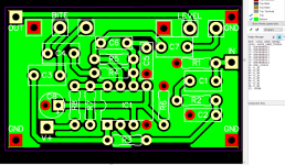
Building like a hundred pedalpcb boards and only two or three from other sources has made me super partial to a clean and organized pcb layout. As I’ve been moving some breadboard circuits to pcbs, I find myself getting super frustrated with this aspect.

Edit:
I’ve edited down my OP in this thread to more accurately reflect where this thread has headed to serve as a broader introduction to the thread for people just joining us.

My original question was more about component organization and aesthetics (cut me some slack, I’m a graphic designer : ) ) which I think of now of as more of an effect of other more important pcb considerations.
 
Last edited:
Check out the videos the dude from effectslayouts.blogspot.com recently did on the topic.

And I think the JMK pedals guy made some very good ones several years back to.

I started building on vero, so the whole this grouped cleanly with that so it looks nice doesn’t really phase me. Keeping the size reasonable and noise down and stuff like that (which I am sure mr PCB takes into account) is more important.
 
I'm not sure you'll find a guide "how to lay out neat looking (PedalPCB style) board" ;).
If you are already familiar with PedalPCB style layout just try to introduce it into your designs. Should be easier with every board you design.
 
I started building on vero, so the whole this grouped cleanly with that so it looks nice doesn’t really phase me.

My entry into building pedals was rehousing something that was in a (imho) super ugly enclosure, and it took a long while to feel like I wasn't just trudging through the circuitry to have fun on the enclosures, I can't shake that introduction sometimes lmao

Check out the videos the dude from effectslayouts.blogspot.com
And I think the JMK pedals guy made some very good ones several years back to.

Thank you so much for the recs @Matmosphere ! Will look into this today on my phone when I should be working.

I'm not sure you'll find a guide "how to lay out neat looking (PedalPCB style) board" ;).
Ah ... shoot! :ROFLMAO: Give it another year or two and I bet there'll be tutorials on cloning the clones!

Thanks for the recs and advice. :)

What is pedal building if not finding new hyper-specific things to obsess over? I need my board laid out as well as a those from a professional with decades of experience, or I may as well not even get the board made! /s
 
Just wondering if anyone could point me in the direction of any resources that talk about pcb layout with that perspective noted

I haven't been able to find a copy of it, but evidently many moons ago R.G. Keen put out a book called PCB Layout For Musical Effects that I see referenced a lot. You used to be able to purchase it at Smallbear, but as far as I can tell it hasn't been available for years.

Robert

 
I've seen some recommendation of the mentioned book but the overall price was a bit high (book + shipping). Could not locate any online preview.
 
I've read the R.G. Keen book. I think you can get most of what is in it from online stuff. The biggest gem in there for me was to layout the PCB following the circuit diagram, i.e., start placing the components from your input and add them to the layout sequentially as you work your way through the circuit. That helps a lot to get connected things to have short traces between them.
 
I've read the R.G. Keen book. I think you can get most of what is in it from online stuff. The biggest gem in there for me was to layout the PCB following the circuit diagram, i.e., start placing the components from your input and add them to the layout sequentially as you work your way through the circuit. That helps a lot to get connected things to have short traces between them.
Yup, exactly this. Keep your schematic open while you're doing placement/layout. I would also add that placement should take at least twice as long as actual routing, because proper placement makes routing easy, whereas no amount of routing can make up for bad placement.
 
There are a lot of considerations when routing circuit boards and often we have to make compromises.
  1. Keep input and output circuits away from each other.
  2. Use a ground plane. Flood fill both sides of a 2-layer board with ground.
  3. No floating islands. Every piece of copper on a circuit board should connect to something.
  4. Keep traces going to the inputs of opamps and transistors short.
  5. If you have a charge pump, locate it in one corner of the board and keep the input circuitry away from the charge pump.
  6. Two dual opamps are easier and cleaner to route that a single quad.
  7. Keep vias to a minimum. They take up space and a clean route won't need very many, if any.
  8. Avoid routing traces thru tight spots, such as between IC pins.
  9. Be generous with ground pads.
  10. Don't be afraid to rip up half of the board to re-route or alter placement.
Engineering is an iterative process. We take our best shot and if it doesn't work out, we take a step back and try something else.
 
Avoid routing traces thru tight spots, such as between IC pins.
I’ve been wondering a lot about this one, because I did it on a couple of layouts that I posted to Reddit for critique, and was told that it’s a bad idea. However, I’ve noticed that PedalPCB boards seem to do it fairly regularly, so I’m not really sure what to believe. When is this ok, and when is it not, and what is the rationale? 3141B05E-B777-4732-BDC2-87D46D878699.png
 
I'm not saying it's absolutely verboten to route traces between IC pads, and in some cases it's the best option. On the Mahayana Drive, all of the pads around the IC are on 0.1" centers, so the IC pads aren't any closer than the resistor pads. When the board is that dense, it's unavoidable. These boards are well made and they have thru-plated holes, so the pads are very robust. If this was a single-sided board, I'd worry about pads that small lifting.

I had heard Reddit was the go-to place for investment counseling, but I had no idea you could get good advice there on PCB design.
 
Great response, Chuck! Of course, I know better than to deal in absolutes, and to take Redditors’ advice/dogma with a grain of salt. But yours is a sound explanation that makes sense to me and helps me to better understand the “why” in addition to the “what”. This is the kind of information I’m looking for, so thanks!

Incidentally, that was another thing I saw a lot of on Reddit: that I should make my pads bigger. Bear in mind that I was using mostly footprints from the default KiCad libraries, which already have larger pads than PedalPCB, Aion, and several others that I could probably think of. I can only assume that these people were either etching their own boards, or at least started out that way and are still using footprints with large pads after moving to farming out their boards to JLCPCb/OshPark/etc.
 
Larger pads are more robust, which is critical on boards that do not have thru-plated holes. Board etching is a tricky process and folks who do it in the garage have a tough time controlling trace width. The automated board fab processes at the production houses produce very consistent results.
 
Sorry to revive this and cabbage on, but there’s some good info in here. I’ve just started to use diptrace. Had a little voltage inverter for positive ground circuits that seems to work.

Anyway, I’m trying a slightly larger circuit and had question about the ground plane. I have through plated holes and the traces and flood are on the bottom layer. Traces are .035” and pads are .080”. All the red pads are ground. Can anyone give me some pointers to make this better?
 

Attachments

  • 35DFB32C-141D-449B-B759-31B1800FE05D.png
    35DFB32C-141D-449B-B759-31B1800FE05D.png
    106.5 KB · Views: 20
You say you have thru-plated holes. Is this a double-sided board, and if so, can you show us the other side?

Also, please post a schematic.
 
You'll probably want to enable "4 spoke" thermals for the copper pour connections, otherwise soldering those pads will be a bit tough.

1642218652711.png
 
Here is the schematic.

A3966E52-BB9D-4186-91F0-31D664997929.png

Here is the top. Yes a two layer board.

1FE4C562-8D9C-4FD4-867A-CA317F3D57E4.png

Here is the bottom with spoked grounds. I left my mouse on the grounds to make them red and the top silkscreen for reference. All the traces and ground fill are on the bottom.

8132AC87-E76F-4E06-A6EC-575E97449140.png
 
Back
Top