Powersound Overdriver Colorsound Help

Zduck

Member
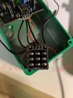
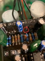
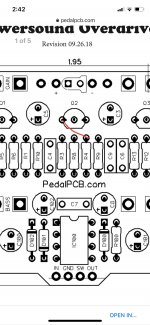
When engaged the volume is really quiet. Bypass doesn’t seem to work at all.

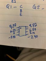
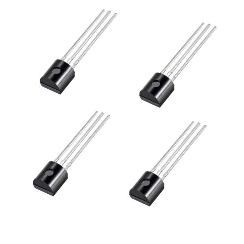
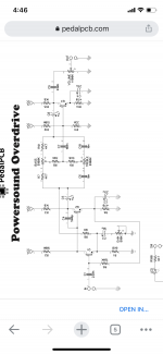
Did I miss anything obvious? I used 2n5088 transistors instead of BC109 as I read they were a modern equivalent. Would that cause a problem or did I put them in backwards? The only other difference from the build instructions is I used 22u caps instead of 25u on c3 and c11. There is voltage on the IC legs and 9-14v on the diodes.

Thanks for any help! I’m fairly new to this!
 

Attachments

  • 73BC6BC4-C338-4E2B-BD9E-4A81888136D1.jpeg
    73BC6BC4-C338-4E2B-BD9E-4A81888136D1.jpeg
    230.1 KB · Views: 30
  • FB788D63-19C5-47AC-AF6E-C2BB23C5816E.jpeg
    FB788D63-19C5-47AC-AF6E-C2BB23C5816E.jpeg
    255.8 KB · Views: 25
  • 3D063854-E4AA-46EF-8334-4C53BC29DB6E.jpeg
    3D063854-E4AA-46EF-8334-4C53BC29DB6E.jpeg
    245.8 KB · Views: 27
  • 0B0B31AE-890D-4EBA-8B25-DCEF38541345.jpeg
    0B0B31AE-890D-4EBA-8B25-DCEF38541345.jpeg
    300.8 KB · Views: 21
What footswitch are you using?
Standard 3pdt on/off footswitch and the pedalpcb true bypass pcb.

I used an audio probe to test things and the input from the input jack has sound but the pad going to the output jack has zero signal. This is when in bypass. This makes no sense to me? The footswitch pcb is soldered on really well.. 🤔
 

Attachments

  • 22888C38-0F17-49C0-9A71-0E7EBC8CC323.jpeg
    22888C38-0F17-49C0-9A71-0E7EBC8CC323.jpeg
    628.8 KB · Views: 8
The first thing I would do is probe volume middle lug 2 to see how strong the signal is coming out then probe your out pad it should be the same, that'll let you know if you're loosing signal before it gets to the out jack and 3PDT and if you have more than one problem it may just be a dry solder joint on your red out wire

You wouldn't get audio on the main pcb OUT pad when the circuits bypassed audio doesn't travel through the circuit in bypass mode you're simply sending you guitar signal IN at lug 2 along the 3PDT jumper between lugs 3 and 9 straight up to lug 8 your OUT jack to your amp (red lines) switched the other way (purple lines, effects mode) you'd send your signal in up to pcb in through the circuit to pcb out and the out jack

You should get bypassed signal regardless of a fault in the circuit

Check your 3PDT lugs with your audio probe in bypass mode and see if you get signal and it's strength on lugs 2, 3,9 and 8 from your description you should have good signal on lug 2 in jack tip so it's just a case of checking the jumper across to and the out jack tip have good connections

3pdt wiring.jpg

With no bypassed signal it has to be either incorrect jack wiring, (can't really see them clearly) faulty switch a dry solder joint somewhere or a short

At a quick check your components look correct can't see R4, 7, 9

Your 3PDT is the correct type hopefully it'll be a nice easy dry solder joint
 
Last edited:
The first thing I would do is probe volume middle lug 2 to see how strong the signal is coming out then probe your out pad it should be the same, that'll let you know if you're loosing signal before it gets to the out jack and 3PDT and if you have more than one problem it may just be a dry solder joint on your red out wire

You wouldn't get audio on the main pcb OUT pad when the circuits bypassed audio doesn't travel through the circuit in bypass mode you're simply sending you guitar signal IN at lug 2 along the 3PDT jumper between lugs 3 and 9 straight up to lug 8 your OUT jack to your amp (red lines) switched the other way (purple lines, effects mode) you'd send your signal in up to pcb in through the circuit to pcb out and the out jack

You should get bypassed signal regardless of a fault in the circuit

Check your 3PDT lugs with your audio probe in bypass mode and see if you get signal and it's strength on lugs 2, 3,9 and 8 from your description you should have good signal on lug 2 in jack tip so it's just a case of checking the jumper across to and the out jack tip have good connections

View attachment 9882

With no bypassed signal it has to be either incorrect jack wiring, (can't really see them clearly) faulty switch a dry solder joint somewhere or a short

At a quick check your components look correct can't see R4, 7, 9
The 2N5088 has the same pinout as the BC109
Your 3PDT is the correct type hopefully it'll be a nice easy dry solder joint
Thanks so much for you suggestions! As for the footswitch, the jacks are 100% soldered correctly, and the lugs on the footswitch are 100% soldered to the pcb really well (and resolded several times). I'm going to chock it up to a bad footswitch... Anyways, since I posted I removed the footswitch from the equation by soldering the jacks straight to the main pcb to try to figure out the low volume problem. Unfortunately, since I hadn't heard back from anyone I stupidly cut out the 2n5088s and resoldered another 3 of them in backwards to see if that fixed the problem. No sound came out at all. Now that you've confirmed they have the same pinout as the BC109 and match the layout of the pcb, I will cut those out and resolder in another set in the proper layout. Would the 22uf caps in c3 and c11 instead of 25uf cause such a volume loss? At full volume it's way below unity. Once I get the trannies in I will probe things and let you know what I found out..thanks!
 
No the cap value wouldn't make a difference electrolytics have a tolerance of + or - 20% so a 22u would be fine, 25u caps were a common value when the original pedal was made these days it's 22u

I wouldn't advise removing anything until you know it's a problem you can easily damage solder pads with too much heat removing and replacing components

Continuity check your switch with your meter to see if it's faulty you should get continuity between the lugs with the purple lines clicked one way and red the other way the 3PDT middle common row should only have continuity with either the top or bottom row

When checking make sure the middle row only has continuity with one or the other and not both

As I say if everything is connected correctly and all solder joints are good you should get bypass signal regardless of a circuit fault

Solder joints may look good but can be dry inside especially if too much solder is used

Unfortunately you appear to have a problem in the circuit and with your bypass

Debugging can be frustrating but you're far better finding the fault rectifying it and moving to the next one

Post your transistor voltages that may indicate something
 
Last edited:
No the cap value wouldn't make a difference electrolytics have a tolerance of + or - 20% so a 22u would be fine, 25u caps were a common value when the original pedal was made these days it's 22u

I wouldn't advise removing anything until you know it's a problem you can easily damage solder pads with too much heat removing and replacing components

Continuity check your switch with your meter to see if it's faulty you should get continuity between the lugs with the purple lines clicked one way and red the other way the 3PDT middle common row should only have continuity with either the top or bottom row

When checking make sure the middle row only has continuity with one or the other and not both

As I say if everything is connected correctly and all solder joints are good you should get bypass signal regardless of a circuit fault

Solder joints may look good but can be dry inside especially if too much solder is used

Unfortunately you appear to have a problem in the circuit and with your bypass

Debugging can be frustrating but you're far better finding the fault rectifying it and moving to the next one

Post your transistor voltages that may indicate something
I just checked the footswitch with my meter and theres NO continuity between lugs 8 and 9! I reflowed some solder on them and still no connection. Faulty switch I guess?
 
Well you were right about replacing the transistors too many times. I think I ruined this pcb. It looks like at least one of the transistor pads has gone missing (Q2 Emitter).

Was it from using the solder sucker too many times? Or from too much heat? Can this pcb be saved? I've already wasted 6 2N5088s on this. Chalking it up as part of the learning process. I have tried transistor sockets before but I find that they dont hold the transistors very well so I stopped using them and just soldered right away.

Here are the voltages I'm getting with a 9.5v power supply plugged in right now:

Q1
E: 0.27
B: 0.08
C: 0.27

Q2
E: 0.08
B: 0.70
C: 0.08

Q3
E: 2.17
B: 2.79
C: 9.40

IC voltages in attached picture.
 

Attachments

  • 152516947_181971243688584_3240169791262996425_n.jpg
    152516947_181971243688584_3240169791262996425_n.jpg
    573.9 KB · Views: 11
  • 152654619_4205371089496085_7808127605016634687_n.jpg
    152654619_4205371089496085_7808127605016634687_n.jpg
    138.7 KB · Views: 11
Possibly too much heat has damaged it internally that'd account for no bypass signal

Did you get audio at volume pot lug 2 with your probe

Yes you can save the pcb simply place a wire jumper on the actual component legs from Q2 emitter to R4 side that connects to C3 +
 
Last edited:
I just checked with a probe and volume pot lug 2 is not getting any guitar signal

I was able to probe the guitar signal at the base of Q1 but no signal on the either outside lugs of Q1. It's coming into Q1 but not going out? I'm new-ish to electronics but shouldn't the signal come into the transistor base and go out the emitter? I had just put in a fresh Q1 transistor so it should be okay.
 
You signal looks like it goes from Q1 collector to Q2 base your Q1 collector voltage is low so check R2 and Q1 solder joints

Reflow for around 4 seconds till you get a nice flow and a good connection between solder pad and component legs / pins

Unfortunately you can also damage transistors with too much heat hopefully that's not the case and its just not conducting correctly because of the voltage so don't heat them for too long

I'm assuming you've put your jumper on at Q2 emitter to R4

Using the schematic I'd check continuity on all transistor pins to make sure no other pads are damaged
 
Last edited:
You signal looks like it goes from Q1 collector to Q2 base your Q1 collector voltage is low so check R2 and Q1 solder joints

Reflow for around 4 seconds till you get a nice flow and a good connection between solder pad and component legs / pins

Unfortunately you can also damage transistors with too much heat hopefully that's not the case and its just not conducting correctly because of the voltage so don't heat them for too long

I'm assuming you've put your jumper on at Q2 emitter to R4

Using the schematic I'd check continuity on all transistor pins to make sure no other pads are damaged
Just to confirm the jumper goes like this?
 

Attachments

  • 32D75017-D806-4534-BA98-7BCE8AF93BDB.jpeg
    32D75017-D806-4534-BA98-7BCE8AF93BDB.jpeg
    338.9 KB · Views: 3
Continuity check all pins to be 100% sure from the shop pcb image in your first post that looks like the collector connected to the 1K8 in the schematic

Powersound.jpg
 
I’m having trouble understanding how the transistors work. There is audio signal coming into the base of Q1 (I checked with an audio probe) that measures .08V. (And it goes to R5 as well). But there’s no audio or continuity to either outside lug of Q1? Do transistors need a certain voltage applied to the base and/or emitter and/or collector in order for it to “open” and the signal to come out the collector? I have .70V and .58V reading on the emitter and collector of Q1.
 

Attachments

  • 95B251B2-4DBF-4622-B129-B9CADC76CE8A.png
    95B251B2-4DBF-4622-B129-B9CADC76CE8A.png
    497.4 KB · Views: 1
  • 5984F0D5-CB1A-4DCC-9C2A-E2E6977221B4.png
    5984F0D5-CB1A-4DCC-9C2A-E2E6977221B4.png
    700 KB · Views: 1
  • 34D16ACD-D051-4F8B-8C49-FD516909DB99.png
    34D16ACD-D051-4F8B-8C49-FD516909DB99.png
    440.2 KB · Views: 1
I was able to google these values for a genuine Colorsound Overdriver:

Genuine Pedal voltages

Battery: 18.84V

Q1 C 6.43V B 3.92V E 3.54V

Q2 C 11.53V B 6.44V E 5.82V

Q3 C 10.19V B 2.77V E 2.23V

Looks my Q1 voltages are way too low.
 
Looking at the shop pcb image the 5088 pinout must be the other way around

The BC109 in the TO92 package per the silkscreen isn't that common in every pinout I checked it's EBC same as a 5088 would be turned that way around or at least it looked that way

But in the pcb image for Q1 the left pin definitely connects to a 100K, Q2 and 3 a 1K8 so that'd be the collector comparing it to the schematic

I've edited out my previous incorrect info so as not to confuse anyone else

Fair enough you may have initially put them in wrong but I'm definitely responsible for you doing it again

I can only apologise, if you can't get the transistors out without further damage I'll get you a new pcb sent out seeing as you're a beginner who did it again because of my incorrect info

You can get transistors out without cutting the legs or damaging them I'll msg you rather than write a novel
 
Hmm so I flipped the 5088s and same voltages on all the legs as when they were the other way around.

The collector (left leg) of Q1 is .70V and the R2+ 10k is also .70V.

Q2 collector is .08V and the R3+ 1.8K is also .08V.

Q3 is 9.70V and R13+ 1.8K is also 9.70V.

That’s telling me that there is continuity between the collectors and the next components and the pads on the resistors haven’t been destroyed if they’re passing voltage correct?

Not getting any signal coming out of the circuit. The last place I can get signal is R5+ 150K and Q1 base. Signals going into the transistor and not coming out, too low voltage?
 
Just to be doubly sure the Q1 pad that you pulled off is it the left or right pin as you look at the pcb

Could you provide a link to the 5088s you purchased too

What voltage do you get both sides of R2
 
Last edited:
Back
Top