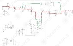
Well, no. You need to probe at various points between In and Out, because there is a connection between C5 at the beginning of the circuit, and C19 at the end.
So having sound at the beginning and at the end of the circuit doesnt mean there aren't any issues in the middle of the signal path.
It just means your connections are good between In and C5, between C5 and C19, and between C19 and Out.
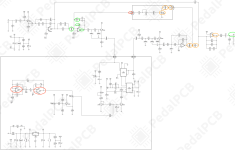
Not having sound at the input of the resonnance section (FB RECV1) is a problem.
It could mean the signal stops between your last checked connection with signal and FB RECV1.
If you have a signal at both ends of R37 but not on the next connector FB RECV1, then there is surely something wrong with that connection.
You will know that connector is fine once you can hear the signal at R42. It's also possible that your connector is misaligned and the pins arent reaching the connector on the daughterboard, it's quite hard to tell sometimes.
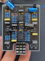
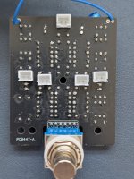
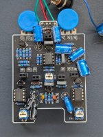
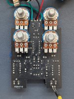
We need to connect perfectly both pcb together before soldering the connectors, to avoid any misalignement.
Maybe it would make your debugging much easier if you just add some extra wires on these connector pads to connect both pcb, and remove them once the effect works. It will at least put aside any doubts about these connectors until the circuit works.
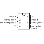
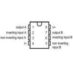
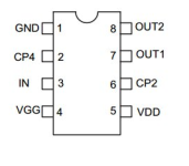
To be able to probe parts like ICs, or check if they are getting the right voltage, you need to look at their pinout to know which leg does what.
You can google it, or use some website like musikding.de.
example : TL22
View attachment 120964
So as you can see, depending on how the IC is implemented in a circuit, you may have some signal on all pins except pin4 (ground) and pin8 (V+).
Looking at the Byzantium schematics, signal enters through pins 5, 6, 2 and 3 and gets out from pin1.
So if you have no signal at all at IC1, you need to find where the signal stops before reaching this IC with your probe, following the schematics.
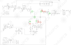
IC1 is part of the BBD section, so first thing is to check if your signal reach C6, near the input of the BBD section.
If it does, keep following the signal until you find where it stops before reaching IC1.
If it doesnt, find where it stops between your last checked connection IC2 pin7 and C6.
Once you find a spot where the signal stops : visual inspection, rework on all pads connected to that spot, use your desoldering pump and start over if needed, continuity test between the parts's legs, and not just the soldering pads, to make sure the connection is good, etc.
Soldering pads are connected to each other with the pcb traces, testing continuity directly on components legs is what matters the most to check the connection.
You can also desolder a resistor's leg and check its value with your multimeter if you think there might be a mistake somewhere.
You cant really check parts like resistors if they are still soldered to the board and connected to other parts, the other connected parts might impair the readings, you need at least one leg out.
Also make sure all trimmers and pots are set at half rotation during your debugging process, so they dont block the signal by being turned off.
Finally, if you really cant get a connection to work as shown on the schematics, the signal stops and nothing can restore the signal path, it could mean there's a problem with the trace or the soldering pad on the pcb.
In that case you can use a piece of wire to connect both parts, as shown on the schematics, in order to fix the signal path.
Edit : About weak signals,
a lower volume level of the signal can be expected depending on where it happens.
The circuit has some fixed clean/wet ratio, it mixes the clean and the modulated signal together which can impact the volume level at various points of the circuit.
If the signal is just a bit lower in volume, up to 50% loss, it should be fine. If it's very faint it could mean there's a problem somewhere, some IC or some transistor not doing its job, or a mistake on a resistor's value for example.