Byzantium Flanger not Flanging

Twinningses

New member
Hi Folks,

Newish builder here and encountering an issue I haven't come across before: I've built the Byzantium Flanger but there's no effect.

Pedal bypass is working fine. When engaged, LED lights up, I get sound, but it's the exact same sound as when the effect is off. The knobs don't alter the sound at all, the trim pots don't alter the sound at all, etc.

I read another thread where people encountered this issue from using the wrong ICs and transistors, but I'm using all the ones to spec.

Interestingly, I don't even here any noise from the ICs that I would expect. Absolutely zero affected signal.

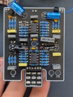
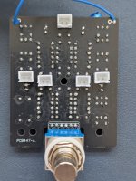
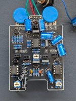
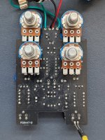
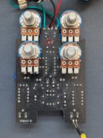
And... forgive my lack of low-profile caps here. I didn't have them for this build and so used what I had and just bent the caps so they still fit between the boards. I've been fairly meticulous to make sure their legs aren't touching things they shouldn't be, so I don't think that's what's causing my issue.

Any and all help very much appreciated.

WhatsApp Image 2026-07-14 at 10.09.06.jpeg
WhatsApp Image 2026-07-14 at 10.09.05.jpeg
WhatsApp Image 2026-07-14 at 10.09.06 (2).jpeg
WhatsApp Image 2026-07-14 at 10.09.06 (1).jpeg
 
Woof. This one can be an intimidating trouble shoot, but I would start by using the continuity function on your meter to verify that the board connections have continuity from one side to the other. Put one probe of the meter to the solder pad of one of the connectors and the other probe to the back side of its mating component on the other board.

Then, verify that each leg of each IC has continuity to its solder pad by touching one lead of the meter to the IC's leg and the other to the back side of the solder pad.

Check that the ground connection exists between both boards.
 
Some of your joints look cold and stressed especially on the 100v caps. the 100u on the top left of the pot board may be shorting it's legs when the boards are squeezed together.
 
Some of your joints look cold and stressed especially on the 100v caps. the 100u on the top left of the pot board may be shorting it's legs when the boards are squeezed together.
Cheers I'll check those particular caps.

For cold joints, you know what my eye for them is not good ever since switching solders. When i was using leaded solder it was super obvious to me when there was a cold joint, but now that I'm using lead-free, I find every joint looks dull and cold.
 
Woof. This one can be an intimidating trouble shoot, but I would start by using the continuity function on your meter to verify that the board connections have continuity from one side to the other. Put one probe of the meter to the solder pad of one of the connectors and the other probe to the back side of its mating component on the other board.

Then, verify that each leg of each IC has continuity to its solder pad by touching one lead of the meter to the IC's leg and the other to the back side of the solder pad.

Check that the ground connection exists between both boards.
Great thanks, will do connectivity checks across everything.

And yea this is a weird one. When I've head connectivity issues before, it's resulted in weak/no signal when engaged... not strong signal with no effect as is currently happening.
 
Hi Folks,

Newish builder here and encountering an issue I haven't come across before: I've built the Byzantium Flanger but there's no effect.

Pedal bypass is working fine. When engaged, LED lights up, I get sound, but it's the exact same sound as when the effect is off. The knobs don't alter the sound at all, the trim pots don't alter the sound at all, etc.

I read another thread where people encountered this issue from using the wrong ICs and transistors, but I'm using all the ones to spec.

Interestingly, I don't even here any noise from the ICs that I would expect. Absolutely zero affected signal.

And... forgive my lack of low-profile caps here. I didn't have them for this build and so used what I had and just bent the caps so they still fit between the boards. I've been fairly meticulous to make sure their legs aren't touching things they shouldn't be, so I don't think that's what's causing my issue.

Any and all help very much appreciated.
1784063619154.jpeg
This one looks like there's not enough solder, other pads also look suspicious to me.

Might be an issue with your soldering technic.

Set the iron around 380 or 400°C, get the tip of the iron in contact with both the pad and the component's leg in order to simultaneously heat both of them for 2 or 3 seconds.
Then put some solder on the pad and remove the tip of the iron upward, along the component's leg, in order to form a nice dome.
You need the right amount of solder, not too much but enough to fill the pad.
If you do it wrong on a pad, use the desoldering pump to start again.
Take your time and give it time to cool down to avoid overheating your pads, and clean the iron's tip often on some piece of dry old sponge, slightly wet.
 
Last edited:
Woof. This one can be an intimidating trouble shoot, but I would start by using the continuity function on your meter to verify that the board connections have continuity from one side to the other. Put one probe of the meter to the solder pad of one of the connectors and the other probe to the back side of its mating component on the other board.

Then, verify that each leg of each IC has continuity to its solder pad by touching one lead of the meter to the IC's leg and the other to the back side of the solder pad.

Check that the ground connection exists between both boards.
Ok thanks for the first set of advice:

I confirm that I have continuity through every leg of the board connections.
I confirm that I have continuity through each IC leg.
I confirm that the ground connection exists between both boards.

I have also reflowed all joints as per @jwin615 's recommendation, as well as checked every cap's legs to ensure they are not shorting.

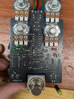
One thing I did notice by happenstance is that both pins on the left board connector (circled in green) have connectivity to ground, where as neither pins on the right board connector (circled in red) have any connectivity to ground. The other three board connectors each have one connection to ground. I need to check the trace to see whether that makes sense but it's now 1am and I've got to call it!

The only other thing I could think of is that where one IC location calls for a "TL022" I have used a "TL022CP" but from what I read that shouldn't make a difference.

Any other advice would be super welcome, thanks in advance!

1784099257013.png
 
If you are sure about your soldering joints and checked with a continuity test all suspicious pads, you can try to narrow it down with an audioprobe.


You can find the signal path by drawing the shortest line from IN to OUT on the schematics.
Circuit powered and switched on, feed the circuit with a signal source connected to the IN jack.
Then probe the pads at various location on the signal path, following the schematics until you found a spot where the signal stops.
Check all connections with continuity tests, make some visual inspections, check components values and orientation, and reflow all pads related to that spot, according to schematics, until you restore the signal path.

You can also make some voltage readings on your transistors and ICs, to make sure they are getting the right voltages.
You can post your readings here if you have some doubts : pin1 = ?,
pin2 = ?, etc.
1784124826338.png
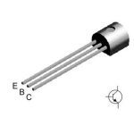
For transistors : E = ?, B = ?, C = ?.
1784126234611.png

EDIT: i cant find the schematics for the Byzantium, does someone have them ?
 
Last edited:
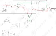
red : quick path that doesnt explore the full circuit, probing here and there will help you locate where the signal stops
and find suspicious aera.

green : quickpath to check if the signal is going in the BBD and Resonnance parts of the circuit, and comes back correctly.
1784127340141.png
 
You might try removing the top board from the bottom one and see if there is a change in sound. Leave them both wired to the footswitch, audio in/out, and power/ground, but separate them from each other (but add a ground wire to the solder pad next to the IN pad and run it to the other board)
 
red : quick path that doesnt explore the full circuit, probing here and there will help you locate where the signal stops
and find suspicious aera.

green : quickpath to check if the signal is going in the BBD and Resonnance parts of the circuit, and comes back correctly.
View attachment 120803
@eh là bas ma thanks for this, I had a chance to audio probe some of this last night.

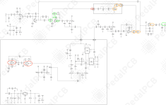
I annotated some of my findings on the below diagram. Green circle means strong audio signal, orange is weak, red is no signal.

First I checked the red line in your path: it was strong audio on the in and out points, which (unless I'm not understanding things) would mean that the signal is connected well through the entire line, even if I detect it as weak at certain other points?

I then checked the upper most green line you drew. While I couldn't detect audio at the FB_RecV1 point, I'm thinking it must be fine if I'm able to detect some sound at the C50k pot and the FB_Send1 point. It's just very, very quiet. Is that a correct interpretation?

I did have a moment to check IC1 and I didn't hear any signal at any point - just some random noise.

Any suggestions on next? Are my interpretations of "weak signal" ok?

1784242516657.png
 
First I checked the red line in your path: it was strong audio on the in and out points, which (unless I'm not understanding things) would mean that the signal is connected well through the entire line, even if I detect it as weak at certain other points?
Well, no. You need to probe at various points between In and Out, because there is a connection between C5 at the beginning of the circuit, and C19 at the end.
So having sound at the beginning and at the end of the circuit doesnt mean there aren't any issues in the middle of the signal path.
It just means your connections are good between In and C5, between C5 and C19, and between C19 and Out.
I then checked the upper most green line you drew. While I couldn't detect audio at the FB_RecV1 point, I'm thinking it must be fine if I'm able to detect some sound at the C50k pot and the FB_Send1 point. It's just very, very quiet. Is that a correct interpretation?
Not having sound at the input of the resonnance section (FB RECV1) is a problem.
It could mean the signal stops between your last checked connection with signal and FB RECV1.
If you have a signal at both ends of R37 but not on the next connector FB RECV1, then there is surely something wrong with that connection.
You will know that connector is fine once you can hear the signal at R42. It's also possible that your connector is misaligned and the pins arent reaching the connector on the daughterboard, it's quite hard to tell sometimes.
We need to connect perfectly both pcb together before soldering the connectors, to avoid any misalignement.

Maybe it would make your debugging much easier if you just add some extra wires on these connector pads to connect both pcb, and remove them once the effect works. It will at least put aside any doubts about these connectors until the circuit works.

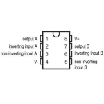
To be able to probe parts like ICs, or check if they are getting the right voltage, you need to look at their pinout to know which leg does what.
You can google it, or use some website like musikding.de.

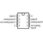
example : TL22
1784321364450.png
So as you can see, depending on how the IC is implemented in a circuit, you may have some signal on all pins except pin4 (ground) and pin8 (V+).
Looking at the Byzantium schematics, signal enters through pins 5, 6, 2 and 3 and gets out from pin1.
So if you have no signal at all at IC1, you need to find where the signal stops before reaching this IC with your probe, following the schematics.

IC1 is part of the BBD section, so first thing is to check if your signal reach C6, near the input of the BBD section.
If it does, keep following the signal until you find where it stops before reaching IC1.
If it doesnt, find where it stops between your last checked connection IC2 pin7 and C6.

Once you find a spot where the signal stops : visual inspection, rework on all pads connected to that spot, use your desoldering pump and start over if needed, continuity test between the parts's legs, and not just the soldering pads, to make sure the connection is good, etc.
Soldering pads are connected to each other with the pcb traces, testing continuity directly on components legs is what matters the most to check the connection.

You can also desolder a resistor's leg and check its value with your multimeter if you think there might be a mistake somewhere.
You cant really check parts like resistors if they are still soldered to the board and connected to other parts, the other connected parts might impair the readings, you need at least one leg out.

Also make sure all trimmers and pots are set at half rotation during your debugging process, so they dont block the signal by being turned off.

Finally, if you really cant get a connection to work as shown on the schematics, the signal stops and nothing can restore the signal path, it could mean there's a problem with the trace or the soldering pad on the pcb.
In that case you can use a piece of wire to connect both parts, as shown on the schematics, in order to fix the signal path.

Edit : About weak signals,
a lower volume level of the signal can be expected depending on where it happens.
The circuit has some fixed clean/wet ratio, it mixes the clean and the modulated signal together which can impact the volume level at various points of the circuit.
If the signal is just a bit lower in volume, up to 50% loss, it should be fine. If it's very faint it could mean there's a problem somewhere, some IC or some transistor not doing its job, or a mistake on a resistor's value for example.

 
Last edited:
Well, no. You need to probe at various points between In and Out, because there is a connection between C5 at the beginning of the circuit, and C19 at the end.
So having sound at the beginning and at the end of the circuit doesnt mean there aren't any issues in the middle of the signal path.
It just means your connections are good between In and C5, between C5 and C19, and between C19 and Out.

Not having sound at the input of the resonnance section (FB RECV1) is a problem.
It could mean the signal stops between your last checked connection with signal and FB RECV1.
If you have a signal at both ends of R37 but not on the next connector FB RECV1, then there is surely something wrong with that connection.
You will know that connector is fine once you can hear the signal at R42. It's also possible that your connector is misaligned and the pins arent reaching the connector on the daughterboard, it's quite hard to tell sometimes.
We need to connect perfectly both pcb together before soldering the connectors, to avoid any misalignement.

Maybe it would make your debugging much easier if you just add some extra wires on these connector pads to connect both pcb, and remove them once the effect works. It will at least put aside any doubts about these connectors until the circuit works.

To be able to probe parts like ICs, or check if they are getting the right voltage, you need to look at their pinout to know which leg does what.
You can google it, or use some website like musikding.de.

example : TL22
View attachment 120964
So as you can see, depending on how the IC is implemented in a circuit, you may have some signal on all pins except pin4 (ground) and pin8 (V+).
Looking at the Byzantium schematics, signal enters through pins 5, 6, 2 and 3 and gets out from pin1.
So if you have no signal at all at IC1, you need to find where the signal stops before reaching this IC with your probe, following the schematics.

IC1 is part of the BBD section, so first thing is to check if your signal reach C6, near the input of the BBD section.
If it does, keep following the signal until you find where it stops before reaching IC1.
If it doesnt, find where it stops between your last checked connection IC2 pin7 and C6.

Once you find a spot where the signal stops : visual inspection, rework on all pads connected to that spot, use your desoldering pump and start over if needed, continuity test between the parts's legs, and not just the soldering pads, to make sure the connection is good, etc.
Soldering pads are connected to each other with the pcb traces, testing continuity directly on components legs is what matters the most to check the connection.

You can also desolder a resistor's leg and check its value with your multimeter if you think there might be a mistake somewhere.
You cant really check parts like resistors if they are still soldered to the board and connected to other parts, the other connected parts might impair the readings, you need at least one leg out.

Also make sure all trimmers and pots are set at half rotation during your debugging process, so they dont block the signal by being turned off.

Finally, if you really cant get a connection to work as shown on the schematics, the signal stops and nothing can restore the signal path, it could mean there's a problem with the trace or the soldering pad on the pcb.
In that case you can use a piece of wire to connect both parts, as shown on the schematics, in order to fix the signal path.

Edit : About weak signals,
a lower volume level of the signal can be expected depending on where it happens.
The circuit has some fixed clean/wet ratio, it mixes the clean and the modulated signal together which can impact the volume level at various points of the circuit.
If the signal is just a bit lower in volume, up to 50% loss, it should be fine. If it's very faint it could mean there's a problem somewhere, some IC or some transistor not doing its job, or a mistake on a resistor's value for example.
@eh là bas ma thank you for your very detailed response above, it was really helpful and very clear to me I'm such a beginner here.

I took some time to read more on the things you suggested. But, I'm still not sure where things are falling apart for me.

So first to say: before building this pedal I did test every component (other than IC and Transistors) with a component tester and confirmed that all components values are measuring correct to spec.

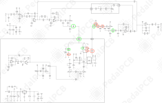
Next, I tried audio-tone probing in the effect section and found that it's not outputting any signal. This would make sense as to why I'm hearing the dry signal but no flanging effect. Green below shows where I heard audio, Red shows no audio:

1785522138344.png

So it looks like IC3 (V3207D) is where my wet signal dies, if I am reading the diagram correctly.

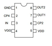
I took your advice and looked up the pinout for V3207D (this is the data sheet):

Screenshot 2026-07-31 at 12.23.31 PM.png

When I put the audio probe specifically on the leg of pin 3 (and confirmed on the solder joint), I hear audio. So audio is going to the chip. But when I put audio on legs 7 and 8 I hear nothing, so audio is not passing through the chip.

So I've found (at least) one error in my build.

Forgive me for using AI, but I'm trying not to consume helpful people's time like yours unnecessarily. According to the problem I'm having with the chip, it suggested the following. Does the below testing protocol make sense to you, or is this gibberish, or should I be doing something else entirely?


No audio on both OUT1 and OUT2 means the delay chip isn't passing signal through. The buckets aren't being clocked, the chip isn't biased/powered, or the chip is dead. The fact that both outputs are dead (not just one) points to something common to the whole chip rather than an output-side problem.

Work through it in this order, since it goes from most common to least:

First confirm the signal is actually reaching IN (pin 3). If it's not, the problem is upstream and the chip is innocent — nothing to do here comes into play. Assuming you do hear clean audio on pin 3, continue.

Check the clock. This is the number one cause. The BBD moves signal bucket-to-bucket only when CP2 (pin 6) and CP4 (pin 2) are receiving the two-phase clock. If the companion clock chip (V3102/MN3102) isn't oscillating, nothing shifts through and both outputs go silent. An audio probe won't reliably confirm the clock because it's usually above hearing range, so use a scope or logic probe on pins 2 and 6 — you want to see activity on both. No clock = no delay, dead outputs.

Check VDD (pin 5). Put a meter on it and confirm it's sitting at your supply voltage (4–10 V) relative to GND. No power, no output.

Check VGG (pin 4). This is the gate bias, and if it's missing or wrong the chip won't conduct signal even with clock and power present. It's normally supplied by the V3102/MN3102 and should measure as a DC voltage close to VDD (roughly 14/15 of it). If VGG reads 0 V or is way off, that's your fault — often a broken trace, cold solder joint, or a dead clock chip (since the same chip usually makes both the clock and VGG).

Check the output pull-down/load resistors. OUT1 and OUT2 need their resistors to ground (the ~5.6k pair in the typical circuit) to develop a signal. If those are missing or the traces are open, you can lose output even with a healthy chip.

If VDD is good, VGG is good, and you've confirmed real clock activity on both pins 2 and 6 with a scope — but still nothing on 7 and 8 — then the V3207 itself is very likely dead and should be replaced.

One clue worth noting: because the same companion chip typically generates both the clock and the VGG bias, a single dead V3102/MN3102 can knock out the clock and VGG at once, which would explain both outputs going silent. That's a common single-point failure, so I'd check that chip early.
 
Back
Top