No wet signal from Ungula Cleft Mod

robertbmillet

New member
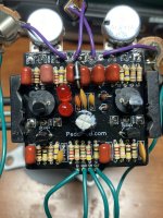
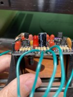
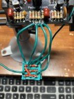
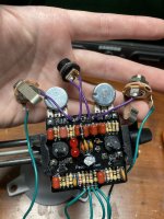
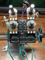
Hello! I have an older revision of the ungula (not sure which, not printed on the board) and it appears quite that some of the pads polarities are labelled opposite from the build guide, which confused me, so I went ahead and soldered negative to the square contacts on the board, which is standard practice but like i said, reversed from the build guide. the project is assembled, but I'm not getting any wet signal. true bypass is working, the main LED is working, and I'm getting 9 volts past D5, which I assume means that power is getting into the rest of the circuit, do i just need to reverse D1-D4? IMG_2108.jpg IMG_2109.jpg IMG_2110.jpg IMG_2111.jpg IMG_2112.jpg
 
If you have one or can get one, a shovel tip for your soldering iron will make taking the pots out a breeze.

1640622315213-png.20379

That beast will heat up all three legs at once, and lekitty-divided your pots will be out and ready for re-orientation.

Otherwise, use a powerful soldersucker (and brass-braid if necessary or preferred) and TAKE YOUR TIME, little bit by little bit.
You don't want to ruin the pads of the PCB by yanking on cold-solder legs.


Check out this post from Robert.
 
Hi All! Thank you for all of your help, I did reverse the positioning of the pots now, and it still isnt working, the circuit is producing popping sounds now, and the volume of the pops is controlled by the volume pot so at least that is working, unfortunately that is the only change, no wet signal still. what would be your recommendations for next steps? Thank you!
 
what are your voltages on your transistors.

Audio probing isna great tool as well just follow the signal til you lose it. I would just check transistor by transistor, once its not there work your way back to where it is. Quick internet search will show you how to make one but i highly recommend the madbeans s-probe board jts worth it.
 
Pots arent insulated, but I have verified that they arent in contact with anything right now. Here are the voltages for the transistors, as im not very good at reading schematics and not sure how to successfully probe
Q1 2N5089
Emitter 1.05
Base 1.38
Collector 8.41

Q2 MPSA13
Emitter .76
Base 1.04
Collector 8.42

Q3 MPSA13
Emitter .01
Base 1.01
Collector 5.98

Q4 2N5089
Emitter 1.18
Base 1.66
Collector 3.40
 
I'm to tired to dig, sorry. But you either have wrong resistor values and/or a bridge. Those voltages seem way off.
Start looking to see if you mixed up 100k and 100R.
 
I measured all of the resistors with my multimeter and it seems like i have a lot that are wildly out of spec? everything was correct in terms of what the resistor value is supposed to be, nothing was out of place, but here are the out of spec readings i received:

R2 measures 85K, should be 100K
R3 measures 130K, should be 470K
R8 measures 84K, should be 100k
R20 measures 110K, should be 390K
R19 measures 80K, should be 100K
R9 measures 130K, should be 490K
R13 measures 80K, should be 100K
R14 measures 125K, should be 490K
R15 measures 13.6, should be 15K
R17 measures 32K, should be 39K

Does this imply something gone wrong in the circuit, or did i just have terrible luck with these resistors?
 
If you have one or can get one, a shovel tip for your soldering iron will make taking the pots out a breeze.

1640622315213-png.20379

That beast will heat up all three legs at once, and lekitty-divided your pots will be out and ready for re-orientation.

Otherwise, use a powerful soldersucker (and brass-braid if necessary or preferred) and TAKE YOUR TIME, little bit by little bit.
You don't want to ruin the pads of the PCB by yanking on cold-solder legs.


Check out this post from Robert.
I wonder if they sell something similar for a Weller WLC100? That looks mighty useful.
 
I measured all of the resistors with my multimeter and it seems like i have a lot that are wildly out of spec? everything was correct in terms of what the resistor value is supposed to be, nothing was out of place, but here are the out of spec readings i received:

R2 measures 85K, should be 100K
R3 measures 130K, should be 470K
R8 measures 84K, should be 100k
R20 measures 110K, should be 390K
R19 measures 80K, should be 100K
R9 measures 130K, should be 490K
R13 measures 80K, should be 100K
R14 measures 125K, should be 490K
R15 measures 13.6, should be 15K
R17 measures 32K, should be 39K

Does this imply something gone wrong in the circuit, or did i just have terrible luck with these resistors?

What Nostradoomus said.
You can't measure in circuit, as other resistors and components may affect whatever you're trying to measure.
You have to look at the colour-bands on each resistor and compare to a colour-chart — also, the colour-bands are directional as some resistors will read as a different value if read backwards from their correct orientation.

brown black black red brown = 10k
brown red black black brown = 120Ω


To hammer home Nostradoomus' point, measuring in circuit is unreliable:
for example resistors in parallel with each other in the circuit will interact and present a reading other than what each separate resistor's value is...

resistrs.gif


I wonder if they sell something similar for a Weller WLC100? That looks mighty useful.

I'm looking for one for a Hakko 888D. Let me know if you find one for mine and
if I see something for the Weller WLC100 in my search, I'll let you know. 🤷‍♂️
 
Last edited:
... what would be your recommendations for next steps? Thank you!
New pics.

Bypass works but no effect when engaged suggests something's up with your 3PDT wiring and/or jack wiring.
Suggestion: Confirm & reflow.

Popping noises ... I'll take a stab without looking at the pics again and suggest maybe a transistor is in backwards or faulty.
I see you're using TO-92 transistors, specs call for 2N1308, a suitable sub is 2N1306 (the 2N130x are TO-5 package) and I've seen MPSA13 as a possible recommendation — What transistors are you using for the clipping stages? Did you check their datasheets for pinout?


NEW PICS would be good, given you've corrected the pot orientation, and please include showing the 3PDT's wiring. Speaking of 3PDTs, it's possible to overcook them when soldering and they become faulty.

Suggest orienting the pics correctly upright for the convenience of comparing to the build docs (I'm using doc rev 11.05.17; ahh but now I see rev 05.04.19 shows the MSA13 as a sub; the ref-des boards shown in each doc are identical).
 
Here are those updated pics, I'm not sure what you mean about the transistors? as far as i can tell they appear to be what the mod calls for.
 

Attachments

  • IMG_2154.jpg
    IMG_2154.jpg
    489 KB · Views: 7
  • IMG_2157.jpg
    IMG_2157.jpg
    382.3 KB · Views: 6
  • IMG_2158.jpg
    IMG_2158.jpg
    367.4 KB · Views: 6
  • IMG_2159.jpg
    IMG_2159.jpg
    469.6 KB · Views: 5
  • IMG_2160.jpg
    IMG_2160.jpg
    457.4 KB · Views: 8
Back
Top