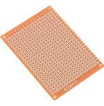
When working with a perf board where the pads are isolated like this (see attached image), is it best to bridge the solder between connecting pads or is it better to bend the leads over and use that wire to make the connection?
Basically. I've only done one perf build, a silicon npn ff. I ended up making traces with spare bits of clipped leads along with the component leads. Though requiring more auxiliary materials, I kinda just prefer etching for single sided boards. Even more than vero. Best of luck, though!
Leads is definitely easier. I tried the bridge of solder blobs method, but it was difficult and ugly. I’ve seen it done well, but I couldn’t get the hang of it.
Using the leads is the better option, unless you plan to replace components. Have a solder sucker pump and wick ready.
Additional and longer connections can be made using insulated wire.
Using the leads is the better option, unless you plan to replace components. Have a solder sucker pump and wick ready.
Additional and longer connections can be made using insulated wire.
What does this mean? “unless you plan to replace components”
Are solder bridges rough on components? Is it because of the prolonged heat while making the bridge or more like solder bridges make for a weaker connection which ruins components?
What does this mean? “unless you plan to replace components”
Are solder bridges rough on components? Is it because of the prolonged heat while making the bridge or more like solder bridges make for a weaker connection which ruins components?
On regular PCBs you just cut the leads after soldering. In case you have to desolder a component that is way easier than on a
perfboard if you bent the remaining leads to make connections to other parts.
With a proper solder iron excessive heat on components isn't a problem.
always bend the lead (or use solid wire), connect that on circle side. No need blob, even 2 component side by side,. So, if you want/need replace component, you just cut lead in between. But i know, almost all perfman rarely do that. We build and leave it is, until broken.
Also, recommended use thick fiber green perf (one or double sided). I choose double because more easy to solder onboard pots, solder from component side.
Dang. I just boxed up my latest perf build, yesterday, and numerous times during the build thought "I need to get a pic of the trace side" — so of course I forgot.
I used a combination of everything: a bit of blob-to-blob (never works well enough, always wants to pool back to a pad), jumpers tacked down at each perf eyelet, jumpers tacked down only at each end, and even an insulated wire running down the middle of the board for the output. Some of the component leads were bent in an L-shape to help form the trace. I planned for and left ends on the offboard-wiring to be bent over and soldered to the next pad/end of row.
Why the hodge-podge of methods? I used what was needed where necessary. For example, the CLR's leads went from the power-in at the top of the board to where the 3PDT's LED-wire pad at the bottom of the board. The CLR was tacked in at 4 points because it was a straight shot at one side of the board without fear of interference from other components and traces.
Here, I've recreated what I did, more-or-less, in the diagram. Note the yellow wire from the pot-leg2 to the output. I haven't marked out all the soldering but the CLR on the left is marked in pink "solder" dots, tacked down in 4 spots. The ground around the perimeter was made with old clipped-leads from PCB builds, and all grounding was tacked down to each of the Perf-Eyelets. I haven't marked out everything I did, solder-dots etc, but you get the idea:
I'll try to get a pic up of this or an older build.