You are using an out of date browser. It may not display this or other websites correctly.
You should upgrade or use an alternative browser.
You should upgrade or use an alternative browser.
Bring out yer Diptrace
- Thread starter Grubb
- Start date
szukalski
Well-known member
You may want to move that IC a little. I think there’s an overlap with the 1n. Also, soldering that pot nearby is going to be a pain.A Spaceman Apollo 7B Layout. I still really don't like laying out ICs with more than 8 pins.. routing power nicely becomes a real pain
JamieJ
Well-known member
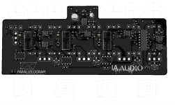
Spent a couple of days playing around with this layout and I think it’s done. It’s 3 parallel FV-1 reverbs (plus an effects loop) with a LM3900 mixer. The second and third reverbs are wet only and have no dry mix. I absolutely maxed out the pin count in the hobbyist DipTrace so I am going to have to hand wire the LEDs. 
I’ve got a couple of custom ordered PedalPCB EEPROMs to try out with it. This all started after I watched this and got obsessed with the parallel reverb sound - TPS is probably my biggest facilitator for GAS.

I’ve got a couple of custom ordered PedalPCB EEPROMs to try out with it. This all started after I watched this and got obsessed with the parallel reverb sound - TPS is probably my biggest facilitator for GAS.
jessenator
Well-known member
falco_femoralis
Well-known member
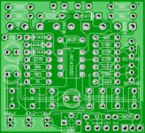
This is my first shot at a PCB - I went for an MXR Il Diavolo, one of the first pedals I really liked. I wanted it to be a certain layout so it can fit it in a double board project I have in mind.
It was difficult to figure out the priority some of the components need when being laid out. Also, the ground pour wasn't cooperating and in my haste I forgot to attach it to the ground net before sending it to JLCPCB. Nice. But the verification checks came back good!
These pics show after I fixed the ground pour debacle


There are a lot of vias.. is that bad?
It was difficult to figure out the priority some of the components need when being laid out. Also, the ground pour wasn't cooperating and in my haste I forgot to attach it to the ground net before sending it to JLCPCB. Nice. But the verification checks came back good!
These pics show after I fixed the ground pour debacle
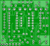
There are a lot of vias.. is that bad?
leadfoot
Well-known member
I try my best to not have them but I haven't seen anything that says having them is bad in a simple audio circuit. I'd be more worried about running audio signal traces right next to power traces. However, I'm sure someone will correct me now that I've said something.There are a lot of vias.. is that bad?
falco_femoralis
Well-known member
Dang, I never even thought of that. I'll try to keep that in mind with the next one. The power is DC and the signal path is low voltage so hopefully it'll be ok!I try my best to not have them but I haven't seen anything that says having them is bad in a simple audio circuit. I'd be more worried about running audio signal traces right next to power traces. However, I'm sure someone will correct me now that I've said something.
Grubb
Well-known member
I love that this thread is still kicking more than 3.5 years after I started it!
I'm popping in to share a build that hasn't quite worked as I hoped. I have been trying to mod the Mach 1 circuit into a distortion on and off for a few years. My latest attempt has a Black Tiger Boost strapped to the front to juice the input, as I liked how my previous prototype sounded with a boost pedal before it. However, with the boost and regular gain controls both above halfway, I get high-pitched oscillation.
I should also remind you that I am approaching this as a tinkerer rather than someone who knows much about electronics!
Schematics:


Layout:

So far I've had two ideas about how to tackle the oscillation, but I'd love to hear if you can think of anything else.
Option 1: Beef up C14. Maybe I selected a bad value for the filter capacitor between VREF and GND.
Option 2: Change R3 to 15K, halving the boost from 20dB to 10dB. The circuit only oscillates with the Pre control up or both Pre and Gain past 12 o'clock, so maybe I could tame it by dropping the gain.
Any other suggestions?
I chucked a Timmy-style Bass control in here too but it is quite subtle, so any ideas about how to give it more impact would be welcome.
Thanks folks!
I'm popping in to share a build that hasn't quite worked as I hoped. I have been trying to mod the Mach 1 circuit into a distortion on and off for a few years. My latest attempt has a Black Tiger Boost strapped to the front to juice the input, as I liked how my previous prototype sounded with a boost pedal before it. However, with the boost and regular gain controls both above halfway, I get high-pitched oscillation.
I should also remind you that I am approaching this as a tinkerer rather than someone who knows much about electronics!
Schematics:

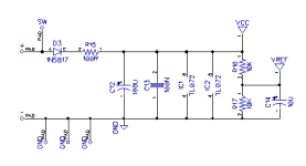
Layout:
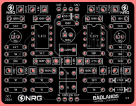
So far I've had two ideas about how to tackle the oscillation, but I'd love to hear if you can think of anything else.
Option 1: Beef up C14. Maybe I selected a bad value for the filter capacitor between VREF and GND.
Option 2: Change R3 to 15K, halving the boost from 20dB to 10dB. The circuit only oscillates with the Pre control up or both Pre and Gain past 12 o'clock, so maybe I could tame it by dropping the gain.
Any other suggestions?
I chucked a Timmy-style Bass control in here too but it is quite subtle, so any ideas about how to give it more impact would be welcome.
Thanks folks!
Last edited:
Grubb
Well-known member
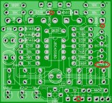
Great job. Plenty of my boards have a lot of vias, generally they aren't an issue. I do try and minimise their use as much as possible because often the layout or component position could be better and the via wasn't actually needed.This is my first shot at a PCB
There are a lot of vias.. is that bad?
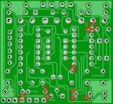
I have marked out some things I would try and avoid on your boards, particularly right-angles in your traces and having the silkscreen overlap with your pads. Otherwise looks great for a first board tbh. Good luck with your project.
leadfoot
Well-known member
A few thoughts..Any other suggestions?
Do clipping diodes to ground instead of Vref.
Add 100n caps at the V+ to gnd at each op amp.
Increase C14 to 47u.
YourGuitarist
Active member
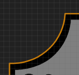
What's the radius on your rounding in the corners?Basically ready for prime time; I'm just extra worryworty with this one. Oh, and I still need PCB art : P
View attachment 106203
View attachment 106204
Robert
Reverse Engineer
There are a lot of vias.. is that bad?
For years I've avoided them like the plague, only using them as a last alternative when I'm on the brink of losing my mind.
Lately, I've started to realize how much cleaner (and less stressful) some of my layouts would have been with a few vias. Technically it's really no different than a trace that passes through the board at a through-hole component pad, and I do that many times in a layout.
I would suggest nudging the silkscreen (or the vias) slightly in cases like this. That value will probably be unreadable.
jessenator
Well-known member
I don't actually knowWhat's the radius on your rounding in the corners?
I think in the earlier days of DIY scene EDA, it was a badge of honor (and economic necessity) to keep a board at 2 layers, and then create a layout without adding vias at all. And while I've got that still stuck in my craw for my own layouts, I'm not going to hold it against anyone! I used vias extensively in my early boards, and there's no shame in it. Sometimes it's also required to link some islands of ground planes, if you've got them in both top and bottom.There are a lot of vias.. is that bad?
If you're doing a lot of SMD work, it's a h*ckin necessity, because you've really only got two layers for the surface components, and then internal layers for supply and ground planes.
szukalski
Well-known member
Monty layout thread is the best thread.I love that this thread is still kicking more than 3.5 years after I started it!
I'm popping in to share a build that hasn't quite worked as I hoped, with the boost and regular gain controls both above halfway, I get high-pitched oscillation.
As a fellow tinkerer with little theoretical knowledge..
Maybe the audio signal is crossing itself between input and output and creating something that you don't want? Your audio path crosses itself alot:
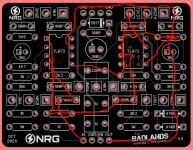
You could change the path across ICs from IC1.1>IC2.1>2.2>1.2 to IC1.1>1.2>2.1>2.2. You should get a nicer flow across the board.
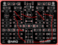
Feck, it may have nothing to help the oscillation, but it's what I would look at.
szukalski
Well-known member
Monty layout thread. Best thread.
Here's an OD series I've been playing with.
The OD-1, Adam Overdrive:

TS-808, Hey let's add a tone control!

Let's crank it a bit with the SD-1

Yamaha won't be left behind, shifting the mid hump down with the OD-10!

And on and on it goes in the pedal world. An overdrive is just an OD-1 with a different tone control.. kinda makes you wonder what else you can do with it. Add a boost? Different diodes? Refine the tone section? What's next? Tune in to find out what will come up in the never-ending OD-1 overdrive collection story!
Here's an OD series I've been playing with.
The OD-1, Adam Overdrive:
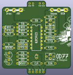
TS-808, Hey let's add a tone control!
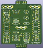
Let's crank it a bit with the SD-1
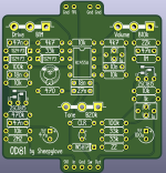
Yamaha won't be left behind, shifting the mid hump down with the OD-10!
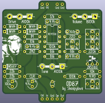
And on and on it goes in the pedal world. An overdrive is just an OD-1 with a different tone control.. kinda makes you wonder what else you can do with it. Add a boost? Different diodes? Refine the tone section? What's next? Tune in to find out what will come up in the never-ending OD-1 overdrive collection story!
YourGuitarist
Active member
FI don't actually knowGrid size is 25 mils here, because the total board dimensions weren't working at 50, which is normally how I like it.
View attachment 109001
I think in the earlier days of DIY scene EDA, it was a badge of honor (and economic necessity) to keep a board at 2 layers, and then create a layout without adding vias at all. And while I've got that still stuck in my craw for my own layouts, I'm not going to hold it against anyone! I used vias extensively in my early boards, and there's no shame in it. Sometimes it's also required to link some islands of ground planes, if you've got them in both top and bottom.
If you're doing a lot of SMD work, it's a h*ckin necessity, because you've really only got two layers for the surface components, and then internal layers for supply and ground planes.
Why use smd/hybrid caps some of the time and the for the rest?
jessenator
Well-known member
Electro caps are often lower profile as SMD, and can have their pins bent to use like like a TH. I think the weird hybrid footprint was just a CYA on my part. Don't have the same problem with film caps right now.Why use smd/hybrid caps some of the time and the for the rest?
falco_femoralis
Well-known member
I've noticed what seems like your earlier layouts are 1590b sized and the component fit is very tight, like on the Seabed Delay. I like these boards as they look great and are very satisfying to build. The (presumably) later boards have components spaced further away from each other. Is there an advantage to placing components further apart?For years I've avoided them like the plague, only using them as a last alternative when I'm on the brink of losing my mind.
Lately, I've started to realize how much cleaner (and less stressful) some of my layouts would have been with a few vias. Technically it's really no different than a trace that passes through the board at a through-hole component pad, and I do that many times in a layout.
I would suggest nudging the silkscreen (or the vias) slightly in cases like this. That value will probably be unreadable.
View attachment 109000
I was playing around with the same circuit I made before, but this time spacing things out in a 1590bb format with everything board mounted. I tried to keep power distribution separate from signal flow and make signal traces as direct as possible.
Also.. I'm smashing tf outta that auto route feature. Are there routes I should place by hand before running the program?
leadfoot
Well-known member
I generally route in, out and power traces to their first connections and then will do the routing of everything myself. If I don't like the way I routed it, I just delete all the traces and try again, then finally, I'll do autoroute to see what it suggests. In the end, I do a mix of auto route and self-route.I've noticed what seems like your earlier layouts are 1590b sized and the component fit is very tight, like on the Seabed Delay. I like these boards as they look great and are very satisfying to build. The (presumably) later boards have components spaced further away from each other. Is there an advantage to placing components further apart?
I was playing around with the same circuit I made before, but this time spacing things out in a 1590bb format with everything board mounted. I tried to keep power distribution separate from signal flow and make signal traces as direct as possible.
Also.. I'm smashing tf outta that auto route feature. Are there routes I should place by hand before running the program?


