Designing my first 2 layer PCB in KiCad which will be manufactured via JLCPCB and looking for guidance on track width.
Is there a rule of thumb people use for selecting track widths? Either for power tracks or signal tracks.
I was able to find this 2015 writeup from MadBean stating:
Is this still considered convention?
Also, how do I identify which connections (or nets) are power and which are signal?
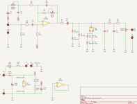
Below is my schematic, I assume the tracks for the signal connections (10 mil) are for connections on the half part of the schematic, and power tracks (24 mil) are for the connections on the lower half of the page.

Is there a rule of thumb people use for selecting track widths? Either for power tracks or signal tracks.
I was able to find this 2015 writeup from MadBean stating:
Power traces are thicker (24mil) whereas audio traces are thin (10mil)
Is this still considered convention?
Also, how do I identify which connections (or nets) are power and which are signal?
Below is my schematic, I assume the tracks for the signal connections (10 mil) are for connections on the half part of the schematic, and power tracks (24 mil) are for the connections on the lower half of the page.

Last edited:

