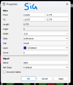
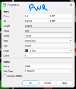
I've been using .3mm and .5mm for signal and power respectively. Not a million miles away. I don't see any reason to go smaller unless it solves a specific layout problem. I'll sometimes run a super fat ground trace but it's probably overkill
Unless I'm doing something like tube heaters, I usually stick around 0.4mm for signal/power. You're never dealing with much current or super high frequencies, so anywhere this ballpark with a sensible layout should be fine
Following up on my ‘Getting Started with PCBA at JLC’ document, I thought I’d create something similar documenting some of my big mistakes and learnings from creating these PCBs.
This isn’t my job or my background, I’m just doing this for fun and it’s all about learning-by-doing (rather, learning-by-making-mistakes-and-starting-over). But hopefully some of my mistakes (especially my repeated mistakes) can become someone else’s learning.
This isn't a "how to design PCBs" post - there's quite a bit of assumed...
Personally I do 10mil where I can get away with it, 8mil if I'm desperate. If you're doing higher current draw in pedals or other you'll have to up it.
I would also download JLC's DRC rules file someone created. Hasn't let me down.