rectifier
Member
So after building a couple of pedalpcb boards I'm asking myself why some 3PDT configurations are chosen over others. Might be a noob question, but I just want to understand it.

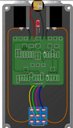
For example, let's look at this board: There are 4 pins In, GND, SW (which acts as a GND for the LED) and Out. The Input and Output jacks are connected with cables. So far so good. With bypass, the input is grounded.
This leads to my first question:
Why is the input grounded, and the output doesn't ? I've seen some 3PDT wirings with both inputs and outputs being grounded. Any benefits to this design over both input and output being grounded?

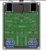
Now with this board the connections are a little bit different. The 3PDT connects with 6 Pins. The Input and Output Jacks are directly connected to the pcb. Input is grounded like in the example before.
Now my questions would be:
- Is this 6 pin design somehow better than the 4 pin design that is basically used on 90% of all the other boards ?
- Ain't the wires from the input and output jacks get some kind of hum or interference with the components on the board? Is this why all the other boards only have 4 pins and rout external cables from the input and output jacks ? Or is this more a matter of taste? I mean with this 6 pin connection and the 3PDT adapter boards the build is much cleaner with no wires floating around.
Thank You
Happy New 2022

For example, let's look at this board: There are 4 pins In, GND, SW (which acts as a GND for the LED) and Out. The Input and Output jacks are connected with cables. So far so good. With bypass, the input is grounded.
This leads to my first question:
Why is the input grounded, and the output doesn't ? I've seen some 3PDT wirings with both inputs and outputs being grounded. Any benefits to this design over both input and output being grounded?

Now with this board the connections are a little bit different. The 3PDT connects with 6 Pins. The Input and Output Jacks are directly connected to the pcb. Input is grounded like in the example before.
Now my questions would be:
- Is this 6 pin design somehow better than the 4 pin design that is basically used on 90% of all the other boards ?
- Ain't the wires from the input and output jacks get some kind of hum or interference with the components on the board? Is this why all the other boards only have 4 pins and rout external cables from the input and output jacks ? Or is this more a matter of taste? I mean with this 6 pin connection and the 3PDT adapter boards the build is much cleaner with no wires floating around.
Thank You
Happy New 2022

