Last edited:
You are using an out of date browser. It may not display this or other websites correctly.
You should upgrade or use an alternative browser.
You should upgrade or use an alternative browser.
Skeptical Buffer Mockup Pedal - Arriving Soon!
- Thread starter music6000
- Start date
- Status
- Not open for further replies.
jhaneyzz
Well-known member
Nice LED placement... At first I thought it was a swollen pickle clone...
iamjackslackof
Well-known member
Been waiting for this one! And I completely approve of the name you picked 
iamjackslackof
Well-known member
It's no ordinary buffer. It's a Elite UNity Amplifier. Which is like a buffer + EQ, but with far better marketing...So @Robert what is this thing? Is it literally just a buffer and some eq? If so their marketing is pretty well it’s just marketing I guess lol
bhcarpenter
Well-known member
Robert
Reverse Engineer
Last edited:
Bricksnbeatles
Member known well
almondcity
Well-known member
I've a random question about this that also relates to 2 knob pcb layouts.
Do you give any thought when laying out the pcb how it will be supported by the switches or pots? Like ideally the switches would be at the center of the board to ensure its physically supporting it. I'm about to build a 2 knob one and I'm a little concerned whether the pots being at the very top of the board are enough to support its weight without overstressing the solder joints
Do you give any thought when laying out the pcb how it will be supported by the switches or pots? Like ideally the switches would be at the center of the board to ensure its physically supporting it. I'm about to build a 2 knob one and I'm a little concerned whether the pots being at the very top of the board are enough to support its weight without overstressing the solder joints
Robert
Reverse Engineer
It's usually not too big of an issue but never hurts to be cautious.
Solid core wire (or rigid pinheaders) at the 3PDT adds stability.
There are various ways to add support if you're concerned about it.
I've added mounting holes for hex standoffs on a few PCBs but I never actually see them used. GuitarPCB has adhesive PCB clips as well.
I (possibly foolishly) leave some of that up to the builder to decide. Everyone does things differently and in some cases (like the Skeptical PCB) the only thing that could be done is to create some wonky control layout and no one wants to see that.
As long as there are no heavy components like a Belton Brick or transformer it's usually not too big of a problem. The ones that bug me are the one-knobbers where the entire assembly can spin around (or twist side to side) in the enclosure.... but again, this can be solved by anchoring to the footswitch or using some form of standoff.
The Battery Box is a good example, it has no hardware whatsoever to anchor it to the enclosure so you use hex standoffs on the top and bottom of the PCB. When the lid is on the enclosure it's snug as a bug and floating at about mid-height. (Just enough to keep the 9V battery in place)
The standoffs don't even have to be fastened to the enclosure because they make direct contact with the top and bottom.

This was just a test fit, I know the jacks haven't been properly drilled.
Solid core wire (or rigid pinheaders) at the 3PDT adds stability.
There are various ways to add support if you're concerned about it.
I've added mounting holes for hex standoffs on a few PCBs but I never actually see them used. GuitarPCB has adhesive PCB clips as well.
I (possibly foolishly) leave some of that up to the builder to decide. Everyone does things differently and in some cases (like the Skeptical PCB) the only thing that could be done is to create some wonky control layout and no one wants to see that.
As long as there are no heavy components like a Belton Brick or transformer it's usually not too big of a problem. The ones that bug me are the one-knobbers where the entire assembly can spin around (or twist side to side) in the enclosure.... but again, this can be solved by anchoring to the footswitch or using some form of standoff.
The Battery Box is a good example, it has no hardware whatsoever to anchor it to the enclosure so you use hex standoffs on the top and bottom of the PCB. When the lid is on the enclosure it's snug as a bug and floating at about mid-height. (Just enough to keep the 9V battery in place)
The standoffs don't even have to be fastened to the enclosure because they make direct contact with the top and bottom.

This was just a test fit, I know the jacks haven't been properly drilled.
Last edited:
Bricksnbeatles
Member known well
Doesn’t appear to, based on the pic of the board on the site. Might be easy enough to hack in, but I couldn’t really say without knowing where the loop is in the circuit or if it has many additional components needed for itLooks sick!
Do we know if it has the effects loop?
Robert
Reverse Engineer
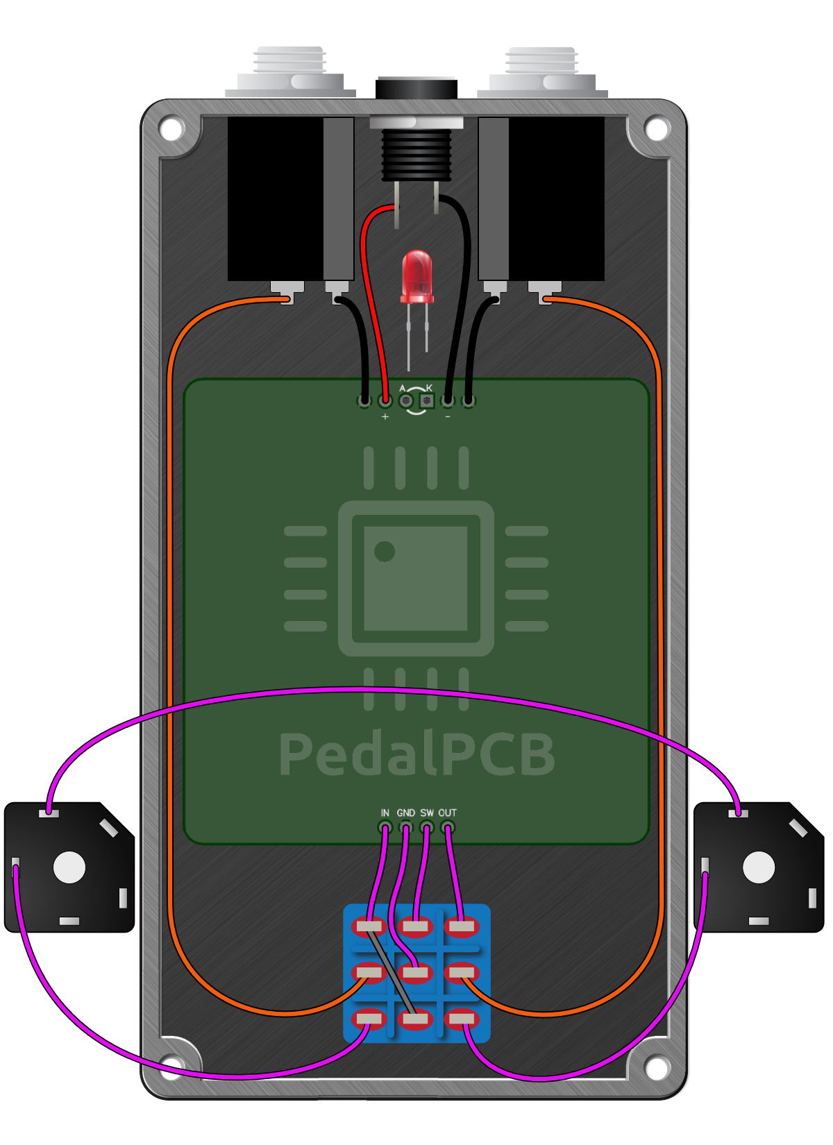
The loop would be wired offboard using a pair of switched jacks, if desired.
It's completely passive, no additional components involved, and only active when the effect is in bypass.
I suppose I could create a breakout board to assist with the wiring, but in this case it's probably easier to just wire it up without one.

It's completely passive, no additional components involved, and only active when the effect is in bypass.
I suppose I could create a breakout board to assist with the wiring, but in this case it's probably easier to just wire it up without one.

Last edited:
Oh yeah I see it now!The loop would be wired offboard using a pair of switched jacks, if desired.
It's completely passive, no additional components involved, and only active when the effect is in bypass.
I suppose I could create a breakout board to assist with the wiring, but in this case it's probably easier to just wire it up without one.

You can put in a stereo jack (1/4" or 1/8") and make it a control port to just plug it in if you want.
Would you have to put the loop’s jacks pretty low like down by the footswitch, or is there room between the PCB and footswitch?The loop would be wired offboard using a pair of switched jacks, if desired.
It's completely passive, no additional components involved, and only active when the effect is in bypass.
I suppose I could create a breakout board to assist with the wiring, but in this case it's probably easier to just wire it up without one.

Or maybe mount some of the electrolytic caps on the other side of the board to make room higher up above the PCB?
Robert
Reverse Engineer
To be fair the "Whatever" power supply is more complex than the signal path itself and has a couple rather pricey components.
We're using more commonly available parts in the charge pump to achieve similar operating voltages, the only catch is that you'll have to power it on a standard 9VDC power supply.
I honestly didn't design the PCB with the loop in mind because it didn't seem like the most useful function in the world to me.
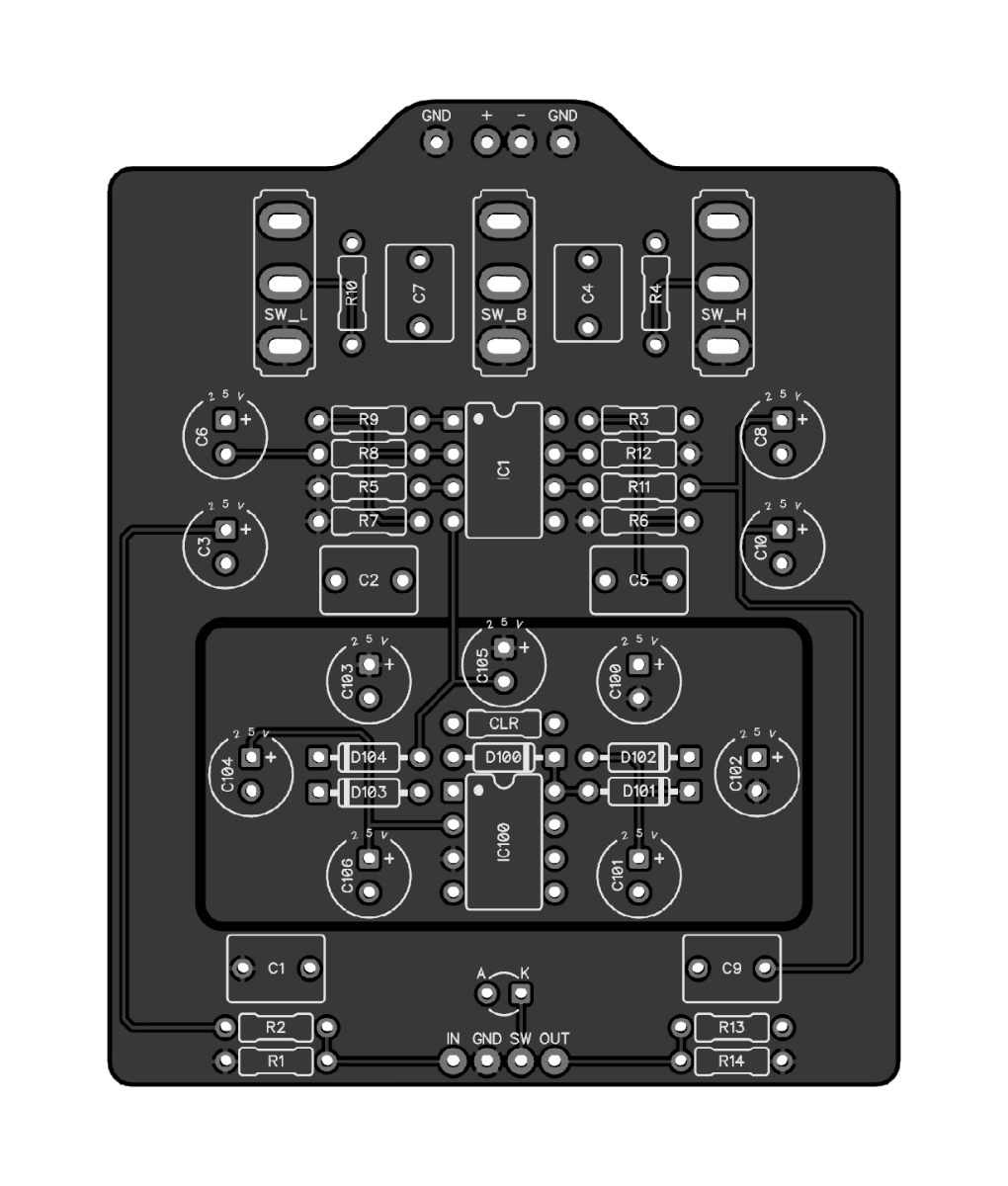
I think it'd be fairly easy to mount the jacks near the footswitch by laying down the two film caps in that area (or even mounting them on the opposite side of the board). That is probably a possibility to push them higher up in the enclosure as well, but I'll look into that when I build the prototype. Worst case scenario it could be built in a 1590BB for those who really want the loop function with all top mounted jacks.
If there turns out to be enough demand for it I could rework the PCB at a later point with the loop in mind.
We're using more commonly available parts in the charge pump to achieve similar operating voltages, the only catch is that you'll have to power it on a standard 9VDC power supply.
Would you have to put the loop’s jacks pretty low like down by the footswitch, or is there room between the PCB and footswitch?
I honestly didn't design the PCB with the loop in mind because it didn't seem like the most useful function in the world to me.
I think it'd be fairly easy to mount the jacks near the footswitch by laying down the two film caps in that area (or even mounting them on the opposite side of the board). That is probably a possibility to push them higher up in the enclosure as well, but I'll look into that when I build the prototype. Worst case scenario it could be built in a 1590BB for those who really want the loop function with all top mounted jacks.
If there turns out to be enough demand for it I could rework the PCB at a later point with the loop in mind.
caspercody
Active member
Can we get the BOM? Would like to add these parts to my next order.
- Status
- Not open for further replies.


