The Protoboard Chronicles: The Replacement Fuzz

Big Monk

Well-known member
So, I can never leave well enough alone.

I went in to change the emitter cap on my hybrid Fuzz Face and all hell broke loose. Crazy ground hum, oscillation, etc. I had an issue with my instrument cable which confused the matter. In the end, I did not really feel like troubleshooting it. I have a few Universal Boards left so I thought I’d go Breadboard to Real Board.

I’m not 100% sure what I’m going for yet but I believe it will be a MK II/Supa with a Silicon Q1 and Q2 and Germanium Q3.
 
Last edited:
What’s a universal board? Can you show a pic? Or is that a stripboard with breadboard-like copper tracks

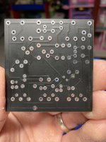
This is the VanderScott Universal Fuzz Board:

C314AE3F-04E8-42AC-BD6C-70F8C2D7C84F.jpeg 1A9E28A0-BD2F-4A17-A990-6C3B5310F1CE.jpeg

It’s not completely universal. It will allow you to build either the Tonebender MK II, Marshall Supafuzz, Tonebender MK 1.5 or Fuzz Face.

It allows for bias trimmers on all transistor slots, an output/Mids trimmer, base to collector caps on all transistor slots, and a base to power resistor for using Silicon transistors in Q1. There is also a Pre-Gain control.

Technically you could do something along the lines of the Ramble FX Twin Bender as well.

I have another iteration planned for this that will serve as the Fuzz 2022 giveaway or “The Fuzz”.

This revision will add slots for emitter resistors on all three transistors, the option to put the input cap before or after the Pre-Gain, a dedicated slot for a cap across the feedback resistor and a few extra components slots for configuring Q1 as a unity gain buffer with adjustable series resistance on the output to the 2nd stage.

I had originally planned on doing 2 more Universal Boards, 1 for the Tonebender MK I types and 1 for the Tonebender MK III types. I still might do that.
 
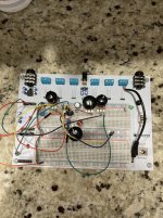
So I had a chance to do a bit or Protoboard if tonight.

I decided to redo the Hybrid Fuzz Face with a few changes:

1.) Make the Q1 bias fixed. 36k locked the collector voltage in at around 1.08 vDC, which is where I had it set.

2.) Tweak the volume pot down to 100k to brighten things up a touch.

3.) Tweak the emitter cap down to 10 uf and keep the input cap down to 0.82 or 1 uf. Not sure yet. It was at 1 uf and I might keep it that way until I see how the rest of the circuit plays out.

4.) Put in a a larger output/Mids trimmer. 470 ohm and 1k combo.

5.) Go for a larger sweep on Q2 bias trimmer. 3 vDC-8.2 vDC depending o. The position of the output/Mids trimmer.

I dialed in the bias voltages tonight and I am traveling to pick up my in-laws at the Albany Airport tomorrow so I probably won’t solder this up until Friday. I need some time to determine feedback bypass, Q1 and Q2 base to collector caps if they are needed.

8B6F5571-355F-499F-87D5-8C8BACB96086.jpeg

Transistor set is an Amperex A115 (hFE = 86) for Q1 and a General Electric 2N169 (hFE = 120) for Q2.

I have 2 boards left and an old Ball Silver enclosure so I maybe throw a full Hybrid MK II together as well.

These are the last 2 Rev. 3 boards I have left and then I’ll make the tweaks for “The Fuzz” or Rev. 4.
 
Do you tend to keep your indicator LED fixed to your board for other builds? Same question but with the power supply jumpers for both boards. Looks great so far!
 
Do you tend to keep your indicator LED fixed to your board for other builds? Same question but with the power supply jumpers for both boards. Looks great so far!

The green is a power indicator. The red is the bypass LED for the circuit.

Yup. I keep all the jumpers in. Also, I have a trim pot between power in and the actual power rail to adjust voltage down on my Snark adapter.
 
Have you thought about doing a ground plane copper pour or are you specifically avoiding it? Defaulting to them on my boards has had a big noticeable reduction in hum and stray noise for me.
 
  • Like
Reactions: fig
Have you thought about doing a ground plane copper pour or are you specifically avoiding it? Defaulting to them on my boards has had a big noticeable reduction in hum and stray noise for me.

Frankly, I’m a neophyte when it comes to PCB design. This was originally a proof of concept that I could even make a functional PCB and that has proved fruitful.

I’m not avoiding it I just have very little practical experience with it!

I’d welcome any tips and I’m always looking to keep noise and hum down. I use DipTrace.

I have only started using them very recently, and only even more recently have become close to happy with some of my pcbs. @Chuck D. Bones laid out a great bullet list that helped me immensely: https://forum.pedalpcb.com/threads/pcb-layout-guidance.8843/post-81358 I went from basically botching every attempt at making an effect pcb to having 3 or 4 that I am content with since digging into everything in that list.

I can post how to do a ground plane fill for a 2 layer pcb when I have the time in an hour or two today but it's very easy in diptrace.

Edit:

I'd be surprised if there are parts of how I'm explaining doing this that can't be done better but I just wanted to give a rough idea. This is also just specifically a ground pour fill.

Basic ground pour fill​

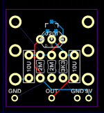
Let's assume this board is entirely routed, with the exception of our ground net. The ratlines here are that net. Blue is top, red is bottom.

1639678369947.png

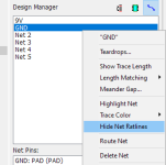
(For the sake of easier routing, I'll hide the ground net's ratlines until the rest is routed, which can be done in the Design Manager's Nets panel)

1639678477744.png

Then we use the tool. We'll use it on both the bottom and top layers, but I'll be walking through doing the top layer before the bottom.
We're gonna snap it to the board outline after it's placed so I just quickly do it oversize of the board

1639678735426.png

For the fill options:
  • In the Pouring tab, check Use Net Clearance.
    • I'll leave other parts of this tab unchanged for now to show why the settings become important.
  • In Connectivity a few things:
    • Connect to Net set to your ground net
    • Hide Net Ratlines to Automatically.
  • Under Border:
    • Check Depending on Board
    • Check Snap to Board Outline
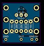
I've dimmed the blue of the top layer to show here why not to Hide All Net Ratlines. Despite being poured, the ground net is broken and the top left corner pad does not make a connection to the bottom pad of 2M, and the bottom pad of the 3K3 does not connect to the bottom right ground pad. You can also confirm this under Verification -> Check Net Connectivity. Using Hide All net ratlines can make you forget that a pour fill does not always route the entire net if there are gaps, which is a fun thing to only realize once you're holding a board in hand.

1639679896155.png

Once we repeat this for the bottom layer, the Ground net might become unbroken without changing anything else - although in this case it did not fix this.

I'll do a combination of a few things at this point:
  • Double check non ground routing and component placement to see if there's an easy way to fix the breaks
    • In this example, they were fixed completely after I realized that the outer pads don't need to be this large for the component
  • I prefer the above but worst case scenario:
    • I'll incrementally creep down the Line Width and Line Spacing in the Pouring tab a bit
    • I'll also change the Border Clearance, or alternatively make the board itself larger.
    • I don't recall the values off the top of my head but it isn't hard to find suggestions for safe values for these.
I've only had a ground pour fill not automatically grab all of the grounds once before I sent off my pcb, but understanding how it can fuck up is knowing how to avoid it. There are tutorials out there that go more in depth that are worth reading, to reiterate this is just a rough cover.
 
Last edited:
I have only started using them very recently, and only even more recently have become close to happy with some of my pcbs. @Chuck D. Bones laid out a great bullet list that helped me immensely: https://forum.pedalpcb.com/threads/pcb-layout-guidance.8843/post-81358 I went from basically botching every attempt at making an effect pcb to having 3 or 4 that I am content with since digging into everything in that list.

I can post how to do a ground plane fill for a 2 layer pcb when I have the time in an hour or two today but it's very easy in diptrace.

Edit:

I'd be surprised if there are parts of how I'm explaining doing this that can't be done better but I just wanted to give a rough idea. This is also just specifically a ground pour fill.

Basic ground pour fill​

Let's assume this board is entirely routed, with the exception of our ground net. The ratlines here are that net. Blue is top, red is bottom.

View attachment 19970

(For the sake of easier routing, I'll hide the ground net's ratlines until the rest is routed, which can be done in the Design Manager's Nets panel)

View attachment 19971

Then we use the tool. We'll use it on both the bottom and top layers, but I'll be walking through doing the top layer before the bottom.
We're gonna snap it to the board outline after it's placed so I just quickly do it oversize of the board

View attachment 19972

For the fill options:
  • In the Pouring tab, check Use Net Clearance.
    • I'll leave other parts of this tab unchanged for now to show why the settings become important.
  • In Connectivity a few things:
    • Connect to Net set to your ground net
    • Hide Net Ratlines to Automatically.
  • Under Border:
    • Check Depending on Board
    • Check Snap to Board Outline
I've dimmed the blue of the top layer to show here why not to Hide All Net Ratlines. Despite being poured, the ground net is broken and the top left corner pad does not make a connection to the bottom pad of 2M, and the bottom pad of the 3K3 does not connect to the bottom right ground pad. You can also confirm this under Verification -> Check Net Connectivity. Using Hide All net ratlines can make you forget that a pour fill does not always route the entire net if there are gaps, which is a fun thing to only realize once you're holding a board in hand.

View attachment 19975

Once we repeat this for the bottom layer, the Ground net might become unbroken without changing anything else - although in this case it did not fix this.

I'll do a combination of a few things at this point:
  • Double check non ground routing and component placement to see if there's an easy way to fix the breaks
    • In this example, they were fixed completely after I realized that the outer pads don't need to be this large for the component
  • I prefer the above but worst case scenario:
    • I'll incrementally creep down the Line Width and Line Spacing in the Pouring tab a bit
    • I'll also change the Border Clearance, or alternatively make the board itself larger.
    • I don't recall the values off the top of my head but it isn't hard to find suggestions for safe values for these.
I've only had a ground pour fill not automatically grab all of the grounds once before I sent off my pcb, but understanding how it can fuck up is knowing how to avoid it. There are tutorials out there that go more in depth that are worth reading, to reiterate this is just a rough cover.

This is great stuff.

Is there a way to do this for manual routing of a board? I don’t currently use both sides and I route everything manually.

You are WAY ahead of my PCB abilities for sure.
 
Last edited:
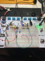
I was able to play this for a few minutes today:

F5B05463-501C-4B04-886C-4A99FA994874.jpeg

As expected, had some noise that was part being on the Protoboard and also just standard Fuzz pedal circuit noise.

I tried to remember the sleep deprived days of my EE undergrad studies and my knowledge of high and low pass filters.

We know the Tonebender MK II uses a cap to ground on the input to roll off highs. I thought that maybe it would also help when combined with my pre gain control to form a high pass filter for eliminating some circuit noise and RF as well.

I subbed in a 2200pf and it worked very well. Still some residual noise but no RF that I could hear at lower volumes. I can try and handle the leftover noise at other points. The good news is that this cap does not seem to affect the treble response but really squashed the noise.

I started with a 1 uf input cap and 10 uf emitter cap. It was a touch mushy at lower volumes so I tweaked down to 0.68 uf for the input and 6.8 uf on the emitter cap and full volume testing will tell me where to go from here.
 
  • Like
Reactions: fig
Just curious as to why you aren't using the terminal blocks instead of shoving those pots in your breadboard?

When I bought the parts for it I mistakenly purchased 2 terminal blocks instead of 3 terminal. I did not have 3 terminal 45 degree blocks but did have 90 degree 3 terminal blocks.

The 90 degree blocks are a pain in the ass to use.

I need to order 6 45 degree term blocks. Until them, I’m using pots on the boards themselves.
 
Coming your way...;)

3mhD6yV.jpg
 
I have only started using them very recently, and only even more recently have become close to happy with some of my pcbs. @Chuck D. Bones laid out a great bullet list that helped me immensely: https://forum.pedalpcb.com/threads/pcb-layout-guidance.8843/post-81358 I went from basically botching every attempt at making an effect pcb to having 3 or 4 that I am content with since digging into everything in that list.

I can post how to do a ground plane fill for a 2 layer pcb when I have the time in an hour or two today but it's very easy in diptrace.

Edit:

I'd be surprised if there are parts of how I'm explaining doing this that can't be done better but I just wanted to give a rough idea. This is also just specifically a ground pour fill.

Basic ground pour fill​

Let's assume this board is entirely routed, with the exception of our ground net. The ratlines here are that net. Blue is top, red is bottom.

View attachment 19970

(For the sake of easier routing, I'll hide the ground net's ratlines until the rest is routed, which can be done in the Design Manager's Nets panel)

View attachment 19971

Then we use the tool. We'll use it on both the bottom and top layers, but I'll be walking through doing the top layer before the bottom.
We're gonna snap it to the board outline after it's placed so I just quickly do it oversize of the board

View attachment 19972

For the fill options:
  • In the Pouring tab, check Use Net Clearance.
    • I'll leave other parts of this tab unchanged for now to show why the settings become important.
  • In Connectivity a few things:
    • Connect to Net set to your ground net
    • Hide Net Ratlines to Automatically.
  • Under Border:
    • Check Depending on Board
    • Check Snap to Board Outline
I've dimmed the blue of the top layer to show here why not to Hide All Net Ratlines. Despite being poured, the ground net is broken and the top left corner pad does not make a connection to the bottom pad of 2M, and the bottom pad of the 3K3 does not connect to the bottom right ground pad. You can also confirm this under Verification -> Check Net Connectivity. Using Hide All net ratlines can make you forget that a pour fill does not always route the entire net if there are gaps, which is a fun thing to only realize once you're holding a board in hand.

View attachment 19975

Once we repeat this for the bottom layer, the Ground net might become unbroken without changing anything else - although in this case it did not fix this.

I'll do a combination of a few things at this point:
  • Double check non ground routing and component placement to see if there's an easy way to fix the breaks
    • In this example, they were fixed completely after I realized that the outer pads don't need to be this large for the component
  • I prefer the above but worst case scenario:
    • I'll incrementally creep down the Line Width and Line Spacing in the Pouring tab a bit
    • I'll also change the Border Clearance, or alternatively make the board itself larger.
    • I don't recall the values off the top of my head but it isn't hard to find suggestions for safe values for these.
I've only had a ground pour fill not automatically grab all of the grounds once before I sent off my pcb, but understanding how it can fuck up is knowing how to avoid it. There are tutorials out there that go more in depth that are worth reading, to reiterate this is just a rough cover.
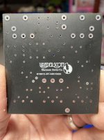
I think there is enough info here for me to do a ground pour even with my simple manual one sided approach.
 
Back
Top