valhalla 6-holes pcb / 3PDT

anatta

New member
Hi!
I'm building valhalla distorsion. I've an issue with cables.
Can you tell me what is the 6 holes of pcb? We have to connectwith 3PDT...
Sorry formy bad english.
 
1: SW2 on Schematic - LED switch
2: GND
3: SW1 on Schematic - This point is shorted to ground in bypass to mute the circuit
4: Buffered bypass output
5: Output jack
6: Effect output

When in Bypass 2 and 3 are connected to mute the circuit, 4 and 5 are connected to send the Buffered bypass output to the output jack.
When Active 1 and 2 are connected to light the LED, 5 and 6 are connected to send the effect output to the output jack.
 
Thank you very much !
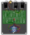
So, I've a problem with 3pdt when weconnect cables like picture (cf. attach file, please). It doesn't work.

Where is the "pcb in" connection or the place of "input jack" on the switch?

I don't understand the footswitch picture.

I've followed allinstructions. Capacitors verified, IC verified, diodes...
Help me, please.
 

Attachments

  • Sans titre 1.jpg
    Sans titre 1.jpg
    156.2 KB · Views: 14
Last edited:
The voltage regulator? If i remember correctly the charge pump get it to 18volts and the regulator drops it back to 12...

The pedal is designed to run on a 12V - 18V power supply, 18V is probably better because of regulator dropout.

The voltage regulator keeps this at a steady 12V which is then inverted by the charge pump to deliver 24V to the opamps. (It's marked +9V and -9V on the schematic, but it's actually +12V and -12V)
 
Back
Top