Viceroy very low gain

Fama

Well-known member
Built up the Viceroy, and it passes signal and sounds somewhat like it should if I dime level, gain and juice and toggle juice to be enabled. Toggle juice to disabled, and it's more of a mid gain thing. Lower either level or gain and it gets way too thin. In short, I don't have as much signal as I should.

First off, I've got some substitutions. Main one being MMBF4393LT1G's for Q1, Q2 and Q3. Second, a 2N5088 for Q4. All of these seem to be lower gain than the normal ones, but my impression was that it shouldn't be a very drastic difference.

At first I had something like 1.3V for Q1, so I desoldered and socketed R6 and R4. Switching out R6 to a 3.3k resistor I now get 5.37V at the drain and 1.63V at the source of Q1 (0V at the gate). Audio probing it it sounds like it amplifies the signal decently, and it's a big improvement over the original with 1.3V.

Q2 is 5.12V and 1.13V for drain and source (gate again at 0). Q3 is 8.36, 5.12V and 2.8V for D/S/G.

I've checked all the caps (except for C2 since I can't see the markings on it - but I don't think it should make a huge difference here?) and I think all the resistors now too, and they match (except for the aforementioned R6). Resoldered all the component joints, didn't see any problems with any of those.

Now, I know Q1 looks horrible because I switched it out for another one thinking it might just be a bum JFET, but it seems to be soldered fine right now from what I can see. The others might look bad due to the flux, but the soldering is ok with those too. Similarly some wires seem like they're not soldered - they are, just from the "wrong" side of the PCB. All of them are firm to tugging with pliers, and there doesn't seem to be grounding or power issues.

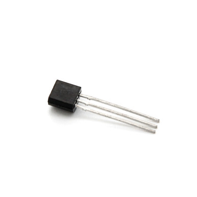
I put in a socket for Q1 in preparation for getting a 2N5457 in the mail sometime in the future, which I might try subbing out, but I've only ever had the SMD parts in it, the socket has been empty the whole time. From what I can see, the pinout should match between the MMBF4393's and the PF5102's (https://datasheet.lcsc.com/lcsc/2304140030_onsemi-MMBF4393LT1G_C152291.pdf, I ordered them from LCSC).

Audio probing the whole way, it sounds like I get decent amplification from Q1, then lose a lot of signal to the bass and treble controls, and then get a lot of amplification from Q2 again - which seems more or less like it should go. I can try to measure dB values if that's helpful, but it's probably not going to be very accurate - I would have to use the audio probe and audio interface for that.

Edit: Handy links:
PF5102 datasheet https://www.mouser.com/datasheet/2/149/pf5102-99964.pdf
 

Attachments

  • DSC_2968.JPG
    DSC_2968.JPG
    504.3 KB · Views: 22
  • DSC_2973.JPG
    DSC_2973.JPG
    307.3 KB · Views: 22
  • DSC_2971.JPG
    DSC_2971.JPG
    387.2 KB · Views: 22
Are your eq controls working at all? C8 looks like it might still have a cold joint, unless you re-soldered after taking that picture.
EQ controls seem to work fine. Bass is not "wafer thin to BASS BOOSTED REMIX" strong, but it's clearly working like a bass control. Treble and presence both also work like I assume they should.
 
I did some more testing, switched R6 out for a trimmer so I could bias Q1 at exactly 5V. That didn't change much, but switching R4 to a 1k made the gain range much more useable.

However, the level is still quite weak. At full blast it's fine, but could go a bit higher, and then 90% of the pot's travel is useless.

Would I need to change R12 to a smaller value to accomplish the same there as with Q1? Or would changing to 2N5457's help? I have tried looking up how to compare JFET specs to figure out which has more gain, but the answer seems to be pretty complex and I don't see the same values in the 2N5457 datasheet I could use to compare.

I just feel like I probably should order PF5102's, but the best I can find is OP Electronics and the shipping is 8.50€ - quite reasonable all things considered, but I don't feel like dropping 15€ on just JFET's for one pedal which might still have something else wrong with it too. Maybe I'll see if I can find some other stuff on the site to justify putting in an order, unless someone else has any other good ideas.
 
The voltage measurements look good, except Q3-G and that's because your DMM is loading down the circuit.

Changing R4 should only have a noticable effect when JUICE is off. Q1 bias is more important when JUICE is on because with JUICE off, Q1 will probably not clip.

I don't know if 2N5457 will work. If you can't find PF5102 (yes, they are scarce these days) then PN4393, MMBF4393 are good subs. J113 might work as well, but you'll probably have to increase R12. I find that running Q3 & Q4 at Id between 1mA and 2mA works well in this pedal.

With TREBLE, BASS & PRESENCE at noon, GAIN & LEVEL dimed and JUICE off, you should be able to drive the 2nd stage to saturation and get 3Vp-p at the output with 200mVp-p input. If that's not happening, then your Viceroy is built wrong.

Here's mine in action. Green: input Blue: output
viceroy.png
 
The voltage measurements look good, except Q3-G and that's because your DMM is loading down the circuit.

Changing R4 should only have a noticable effect when JUICE is off. Q1 bias is more important when JUICE is on because with JUICE off, Q1 will probably not clip.

I don't know if 2N5457 will work. If you can't find PF5102 (yes, they are scarce these days) then PN4393, MMBF4393 are good subs. J113 might work as well, but you'll probably have to increase R12. I find that running Q3 & Q4 at Id between 1mA and 2mA works well in this pedal.

With TREBLE, BASS & PRESENCE at noon, GAIN & LEVEL dimed and JUICE off, you should be able to drive the 2nd stage to saturation and get 3Vp-p at the output with 200mVp-p input. If that's not happening, then your Viceroy is built wrong.

Here's mine in action. Green: input Blue: output
View attachment 64412
I think with Q1 at 5V and R4 at 1k I can saturate Q2. But the output level is still too weak. So I assume it has to be something past that.

I did use MMBF4393, so I guess that part should be fine. From what I gathered, the "Forward Transfer Conductance" is sort of what I could use to maybe compare JFET gain levels (although it's more complex than that), and the PF5102 has 11,000 μmhous while the MMBF4393 has a "Typical Forward Transfer Admittance" of 6,000 to 8,000 at Id of 1-2mA. Assuming conductance and admittance are the same (I don't even know if they are), It's sort of a big difference, but not amazingly huge, so not sure if it should make this big of a difference. I'm also not sure how I would measure my Id here.

Would Q4 being a 5088 instead of 5089 make any difference here? I could switch it out if it helps.

The other thing I'm thinking of is switching R12 out to a different value. I could socket that one too, or put a trimmer in.

The third alternative is of course that something is built wrong, but I'm having a hard time thinking what it could be that lets signal through, and all the controls work more or less correctly (I guess level being the exception here), just that there's too little output. Maybe I'll double check that the pots are all correct values too.
 
Make sure your board is very clean around Q2-Q4. The impedance at Q2-D is very high and any leakage from flux residue, moisture or other contaminants will reduce the gain of the 2nd stage. We need a high HFE transistor for Q4 for the same reason. you can even use an MPS-A13 Darlington.

An incorrect component value could very well let the circuit work, but not perform well.

The Forward Transfer Conductance is the same as Transconductance, which is the DC gain of the JFET. It is usually specified at Vgs = 0, which is the same as running the JFET at at Idss. It's a test condition that produces the maximum gain, but is not an operating condition you'd expect to see in a practical circuit. Forward Transfer Admittance is the AC gain. At audio frequencies, is it the same as Transconductance.
Here are some transconductance values that I measured on a few JFETs running at 1mA:
PN4393: 3.9mS
PF5102: 3.9mS
J113: 4.0mS
2N5457: 2.6mS
Like Vp & Idss, there is a large amount of part-to-part variation within the same part number.
The gain of the 2nd stage is strongly influenced by the Output Conductance of Q2 & Q3. Smaller is better. I have not measured it and not all datasheets specify it. Again, large part-to-part variation.

Best bet is to socket the JFETs or breadboard the circuit so you can audition the JFETs.

I think you'll find that changing R12 has little effect unless you go to extreme values.

If you're doing all of this experimentation / troubleshooting on a PCB, then it won't be long before the traces start peeling off.
Ok, thanks. I think this is my plan now:

1.) Clean out all the flux around the JFET's.
2.) Desolder Q4 and socket it, try out a 2N5089 or MPSA13 there (I have both).
3.) If those won't help, then I'll probably desolder Q1-3 and socket them instead and try out alternatives. I have some J113's, I took it as "might have to increase R12 because otherwise it will be too high gain", so maybe I'll socket R12 while I'm at it.
4.) If those won't help I'll look into ordering PF5102's, I take it MMBF4393's should work but socketing them is much more of a pain (I have some adapter boards, but those are harder on the sockets I feel plus much more effort). Alternatively I read on some other thread about sockets for SMD JFETs and thought that I could maybe do a testing system for SMD JFET's using that, just soldering some wires into it so I could plug it into the through hole socket and see how the JFETs work in an actual circuit.

Lots of sockets involved, but like you said, I can't keep experimenting on the PCB otherwise for long before it stops working. I know sockets won't last forever either, but even if they work a bit badly, once I find the parts that work I can solder those into the sockets and then they should be pretty reliable.
 
You don't necessarily need to change R12. Changing it by 2x either up or down won't have much effect on gain. I shoot for Id in the 1mA to 2mA range, but this circuit will work fine at 5mA or 10mA. J113 tend to have higher Vp than PF5102, but not enough to warrant messing with R12. Try it if you like and see for yourself.

Mouser stocks J113 & PN4393, so you don't need to mess with SMD sockets or adapter boards.

But first, do another visual inspection and look for incorrect part values, including the pots.
 
Pots were all correct, at least according to what's written on the pots themselves and on the PCB.

1.) Cleaned out the flux with isopropyl alcohol, no change.
2.) Desoldered Q4 and switched it out for a 2N5089, no change.
3.) Took out Q1-3 and added sockets for Q2-3 (1 already had a socket installed), measured some of my J113's (I just have the cheapo TC-1 so not sure how accurate it is, if at all) and picked ones which showed Id of 1.2mA (range was from 0.9 to 1.2 for the ones I tested). Put them in, I checked the pinout with the TC-1 too so should be fine. Biased Q1 to 5.02V (0.83V on source). Q2 is 5V and 0.78V, respectively.

It's a little bit improved now - with the juice switch toggled on and pretending it's not an option at all, it almost feels like it could be correct. But there's something about the sound that doesn't quite seem correct to me, and with Juice toggled off, gain and level both at noon is a bit under unity - I really need to crank the gain for it to work as it should.

There's clearly something wrong with my build, but I've run out of steam for now. I guess the next step is checking all sorts of connectivity, are things that are supposed to go to ground actually going to ground and vice versa. Probably do another check of the resistors too at some point because that is very boring stuff - although I'm starting to learn the color bands a little bit now.
 
I recently had a PCB (not from PPCB) where I was having connectivity issues, despite 5 decades of soldering experience + quality solder. I had measured each component before installing it to ensure it was the right value, and after completion went back and re-checked every component and made sure it was correct. Realizing that I likely had a connectivity issue (bad solder joint), I then visually re-checked each joint with a magnifier + performed extensive DMM testing, but could not find the bugger(s). Sometimes a solder joint will incorporate a small oxide or schmutz layer that acts as a tiny low-voltage diode in the circuit, but you won't find it with a DMM because it's measuring voltage biases the diode into conduction. (You can try using a large series resistor with your DMM to reduce the voltage on the connection you're testing, but some bad joints can still be fricking tough to find - Murphy was an optimist, right?)

Anyway, so I finally pulled out my trusty old 8 oz container of Superior No. 30 SuperSafe liquid soldering flux (https://superiorflux.com/products/superior-no-30-supersafe-soldering-flux/) which I used in my prior research life, and lightly put tiny drops on each PCB connection before resoldering them - and it totally fixed my issues. Superior Supersafe #30 is a totally non-corrosive flux, rinses off completely with water or isopropyl, and I highly recommend it. I know 'flux' is often rightfully considered a 4-letter word, as most of them are evil - but this stuff is totally different as it's so safe for electronics. (Still wash your hands and don't drink it, of course.) It's designed for and widely used in PCB assembly plants + research labs because it's so gentle on electronic components. It may be a little hard to find, but it's great stuff.

(I've only used the blue liquid form of No. 30, but it's also available as a paste.)
 
Last edited:
I recently had a PCB (not from PPCB) where I was having connectivity issues, despite 5 decades of soldering experience + quality solder. I had measured each component before installing it to ensure it was the right value, and after completion went back and re-checked every component and made sure it was correct. Realizing that I likely had a connectivity issue (bad solder joint), I then visually re-checked each joint with a magnifier + performed extensive DMM testing, but could not find the bugger(s). Sometimes a solder joint will incorporate a small oxide or schmutz layer that acts as a tiny low-voltage diode in the circuit, but you won't find it with a DMM because it's measuring voltage biases the diode into conduction. (You can try using a large series resistor with your DMM to reduce the voltage on the connection you're testing, but some bad joints can still be fricking tough to find - Murphy was an optimist, right?)

Anyway, so I finally pulled out my trusty old 8 oz container of Superior No. 30 SuperSafe liquid soldering flux (https://superiorflux.com/products/superior-no-30-supersafe-soldering-flux/) which I used in my prior research life, and lightly put tiny drops on each PCB connection before resoldering them - and it totally fixed my issues. Superior Supersafe #30 is a totally non-corrosive flux, rinses off completely with water or isopropyl, and I highly recommend it. I know 'flux' is often rightfully considered a 4-letter word, as most of them are evil - but this stuff is totally different as it's so safe for electronics. (Still wash your hands and don't drink it, of course.) It's designed for and widely used in PCB assembly plants + research labs because it's so gentle on electronic components. It may be a little hard to find, but it's great stuff.

(I've only used the blue liquid form of No. 30, but it's also available as a paste.)
Thanks, looks like I might not be able to get that one in Finland, I only have some very basic solid flux, but I might give it a try with that.
 
Thanks, looks like I might not be able to get that one in Finland, I only have some very basic solid flux, but I might give it a try with that.
Fama - good luck. Just don't use any flux with corrosive components, especially zinc chloride or ammonium chloride. They are very tough to fully remove, and the will corrode the circuit in months/years to come. Use a fine brush or toothpick to put the smallest amount on the contact, you don't want it getting elsewhere.
 
Fama - good luck. Just don't use any flux with corrosive components, especially zinc chloride or ammonium chloride. They are very tough to fully remove, and the will corrode the circuit in months/years to come. Use a fine brush or toothpick to put the smallest amount on the contact, you don't want it getting elsewhere.
The one I have is SRA #135 flux, no zinc or ammonium chloride. The instructions on the back of the puck also say to "remove residue with a rag", which I didn't know is an industry term but I guess you learn something new every day!
 
Well, did a full resoldering with flux in every component joint and also resoldered all the pots. I'm not sure if it did anything, or if spending some time away from playing it made it sound slightly better for me, but I think I'm done tinkering with the pedal now.

I suspect I might still have a bit too little volume overall (unless J113's should have lower volume here), but as long as I run level at around 3'o'clock (which is over unity, but not very loud) and gain around 2'o'clock I can get a nice slightly overdriven sound that works well for chords, and toggling the juice (with the juice pot dimed) gets me a nice high gain rhythm/lead tone. So it works for me now - usually I run volume around noon or a bit over in my pedals, and usually not too high on the gain, so something still feels off... but at least it seems to work ok for me right now.

I'll maybe look into getting PF5102's at some point if I'm doing an order in some store where they stock them, but it's fine like this.

I guess I'll mark it solved now?
 
Back
Top