MBFX
Well-known member
Hi everyone! I have graduated from putting together purchased PCBs to assembling my own circuits on breadboards, and I am trying to learn how signal flow works.

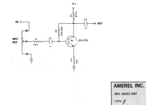
Above is the schematic for a booster I found online just now. I also built an LPB-1 and a Fuzz Face last night. I noticed that all three effects have the signal output flowing from the collector of the transistors, instead of from the emitter like I would expect. Why is that? It seems wrong - the signal should come from the emitter, right? That's the way the arrow points! I realize I am wrong, I just don't understand why.
If someone is feeling particularly kind, I have a few more questions too:
The AC signal from the pickups goes from IN to MPC POT to ground via lugs 1 and 3 of the pot. Lug 2 of the pot is the wiper, and that goes to a 120K resistor. Why is that - doesn't this make the already tiny input signal even smaller?
From the 120K resistor, we connect to a capacitor. I can't really read the value, .1uf maybe? Kinda looks like a 2, but that would be a weird value. Anyway, is this input capacitor used for keeping 9VDC power from flowing back to the input?
The circuit branches off here, with a lead to the base of the transistor, and a lead to a 2.2M resistor. The input goes to the Base to be amplified and sent out of the Emitter, is that correct? If so, that links to my initial question.
The 2.2M resistor connects to a 4.7K resistor and the collector of Q1, both of which connect to +9VDC. So, the collector gets a lot more of the +9VDC current than the base, which is how a transistor is supposed to amplify out of the emitter. Is that correct?
The emitter goes straight to ground through a 470R resistor. By now, kind reader, you've already told me why. Thank you!
The output capacitor, .1uf, is also for DC-blocking. Is that correct?

