Digital BBD concept looking for comments and beta testers

Seems like someone must already make a 9-18V to +5,+3.3 converter that is reasonably quiet and filtered (and not a linear regulator that would itself consume a lot of power).
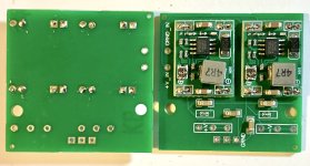
FWIW, I found these neat little BC modules that will accept +4.5V to +24V and deliver +0.8V to +20V, adjustable with a tiny trimpot. Their output ripple is less than 30mV and the switching frequency is typically 1MHz. We've been using them in a dual rail configuration to deliver ±6V at over 500mA for a Rockman X100 project we've been working on. (see attached image)

Wiring diagram . . . . . . . . . . . . . . . . . . . . The PCB we developed for mounting two of the MP1584EN BC modules . . . .
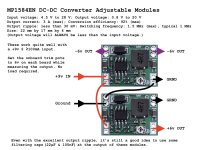
BC_Modules_Dual-Rail.jpg . . . . V2_BC_Modules_00.jpg
 
Something like the XP Power ISV0212S05 for the 5v

Then run a IES0205S3V3 or the like off the 5v line for the 3.3vdc

Sleeping on it, it seems like leaving the Vsources to the designer is more ideal though. That allows integration without redundant power conversion saving space and cost in the end. This will all be ground up designs anyhow, not a retrofit.

On a sperate note, will/would this have a digital link/out function (and clock) for linking multiples, or will the signal need to pass the additional ADDA stages? Just curious.
Yeah I was thinking along these lines (a buck converter for 5V, then a linear regulator for 5->3.3). I am hoping to remove the need for 5V so the module would require only 3.3V. That would simplify things and reduce overall system cost (although may raise the cost of the DBBD a bit). I get that this is for new designs, but if it is the only device in (say) a pedal that needs 3.3V it would help the designer to include it onboard. Food for thought.

On the linking, yes my intent is that they will be digitally linkable to build virtually any length delay line with no degradation in fidelity.
 
Thinking more, 0-5v CV may be better. Doesn't modular run off 0-5?
Also, in the pedal world, the tappy/tapflo tap tempo works on 5v and that's the best/only diy TT I know.
If one could integrate that for tap tempo, wouldn't be a bad idea.
So. 5v only operation would be ideal, and shrink pin count.
Also, easier for the end designer/creator.
 
Thinking more, 0-5v CV may be better. Doesn't modular run off 0-5?
The Eurorack power standard(s) are a bit of a mess, but generally specifies +/-12V with optional +5V. Some have the +5, some don't. The 10-pin connector configuration does not even have pins for +5V at all. So cannot assume 5V is available in Eurorack systems. Many modules that need +5 have an onboard regulator to derive it from +12V.
Also, in the pedal world, the tappy/tapflo tap tempo works on 5v and that's the best/only diy TT I know.
If one could integrate that for tap tempo, wouldn't be a bad idea.
Hummm, I had not considered it, but since you mention tap tempo, we could support that on the module itself to set the overall delay time.
So. 5v only operation would be ideal, and shrink pin count.
Also, easier for the end designer/creator.
This makes sense given the idea that if there is a low voltage supply, it is more likely to be 5V than 3.3V. If there is not one, the system designer must supply +5V, and there are a wealth of options to do it with 9-18V sources. On the down side, we depend on the system designer to create a reasonably clean and reliable 5V rail.
 
Making progress on prototype design and a question came up that we could use some input on...

Is a 'bypass' feature really useful (e.g. an input pin 0=bypass, 1=normal delay)? A real BBD has a minimum delay based on max clock frequency, there is no zero-delay or bypass unless you build it yourself. So we can do a simple digital bypass which results in delay of about 0.8ms, easy peezy. With more work we might get that down to 0.3ms. With lots more work and more components on the board we might get it down to 0.02ms. Is it worth it? Seems like most pedal designs will have a bypass design that completely bypasses the entire circuit, so is there any usefulness to the delay line having a bypass itself?
I wouldn't bother going too deep on a bypass, personally.
 
aye, why eat real estate for important parts like voltage regulation and mono/stereo output, when an off board switch the builder can place themselves has been doing the job for decades.
 
I don't believe any delay, in this use case, that is under a millisecond is all that useful u less the designer needs some crazy specific comb filtering.
 
Preliminary (Prototype) Pinout

ConnPinNameFunction
11GNDGround
12VC_MSCALERVC master scaler: Sets full-scale delay for all delay outputs. 0V=0 delay, 3.3V=660ms delay.
13VC_DELAY0VC output 0 delay. 0V=0 delay, 3.3V = full scale delay as defined by VC_MSCALER.
14VC_DELAY1VC output 1 delay. 0V=0 delay, 3.3V = full scale delay as defined by VC_MSCALER.
15VC_DELAY2VC output 2 delay. 0V=0 delay, 3.3V = full scale delay as defined by VC_MSCALER.
16VC_DELAY3VC output 3 delay. 0V=0 delay, 3.3V = full scale delay as defined by VC_MSCALER.
17VC_MIXVC mixer control feedback mix level, 0V=no feedback, 3.3V = 100% feedback. Mixer is additive.
18N.C.
19nBYPASS, pullupWhen logic level 1 (or N.C.) the delay operates in normal mode. Logic level 0 all outputs are zero delay.
110-16N.C.Future use
117REF_5V
  • Using +5V external supply: This pin is +5V input supply. Jumper EN_33 is installed to enable onboard 3.3V regulator. REF_3V3 is +3.3V output reference, 200mA max draw.
  • +3.3V external supply: This pin is N.C. Jumper EN_33 is removed and REV_3V3 is +3.3V input supply.
118CLIPPINGOutput logic level 0 in normal operation, logic level 1 when clipping is detected. This also drives the on-board clipping LED when the CLIP_LED_EN jumper is installed. If this is used to drive an external LED, the CLIP_LED_EN jumper should be removed and this pin can source up to 10mA and is current limited with a 330R.
119TT_INTap tempo input (future)
120REF_3V3
  • Using +5V external supply: Jumper EN_33 is installed and this pin is a 3.3V output reference (200mA max).
  • +3.3V external supply: Jumper EN_33 is removed and this pin is a 3.3V 600mA input supply.
21GNDGround
22AUDIO_INAnalog audio signal input, 3.3V max
23FB_INAnalog audio feedback signal, 3.3V max. This will be mixed with the AUDIO_IN as controlled by VC_MIX.
24N.C.
25DELAY0_OUTAnalog audio delay 0 output. This output is delayed by VC_DELAY0 and VC_MSCALER.
26DELAY1_OUTAnalog audio delay 1 output. This output is delayed by VC_DELAY1 and VC_MSCALER.
27DELAY2_OUTAnalog audio delay 2 output. This output is delayed by VC_DELAY2 and VC_MSCALER.
28DELAY3_OUTAnalog audio delay 3 output. This output is delayed by VC_DELAY3 and VC_MSCALER.
29N.C.
210N.C.
211-12N.C.Future use
213LINK_INN.C. on single modules or first module in a multi-module configuration. Connected to the upstream module’s LINK_OUT in multi-module configurations.
214LINK_OUTN.C on single modules or last module in a multi-module configuration. Connected to downstream module’s LINK_IN in multi-module configurations.
215LINK_BUS1N.C. on single modules. Connected to all module’s LINK_BUS1 pins in multi-module configurations.
216LINK_BUS2N.C. on single modules. Connected to all module’s LINK_BUS2 pins in multi-module configurations.
217-20N.C.
 
Jumpers

NameFunction
EN_3V3When installed: Enables the onboard 3.3V regulator. External +5V supply must be applied to REF_5V pin and REF_3V3 pin is +3.3V reference output (200mA max).

When removed: Disables the onboard 3.3V regulator. External +3.3V supply must be applied to REF_3V3 and REF_5V is N.C.
CLIP_LED_ENInstalled: Onboard clipping LED is enabled. CLIPPING output pin can source minimal current (e.g. logic gates, etc).

Removed: Onboard clipping LED is disabled, CLIPPING output can source/sink 10mA max (current limited by onboard 330R).
MASTER_SLAVE
(2 position)
MASTER position: This module is either a single, or the first in a multi-module configuration.

SLAVE position: This module is part of a multi-module configuration and is not the first in the chain.
PGM
(4 jumpers)
Defines 1 of 16 possible firmware programs to be used.
 
Firmware Programs (PGM jumpers)

ProgramDescription
01 delay line, 4 taps, 660ms max delay
12 delay lines, 2 taps each, 330ms max delay each. VC_MSCALER defines full scale delay for all delay lines. Each tap in each line is independently controlled.
24 delay lines, 1 tap each, 165ms max delay each. VC_MSCALER defines full scale delay for all delay lines. Each tap in each line is independently controlled.
3Same as #1 except the delay times are linked (e.g. a single VC defines the delay of tap #1 on both lines, another VC defines the delay of tap #2 on both lines).
4Same as #2 with linked delay VCs.
5-15Future use
 
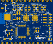
Beta test PCBs are in production! Due to parts shortages we can only get them partly assembled, we will need to finish soldering some of the components by hand. Currently the PCB design is about 2" x 1.7", I expect the final design to be smaller -- we did not spend a lot of time optimizing layout and we will use smaller jumper blocks and other components in the production design.

1698507958120.png

The PCB uses castellated holes so it can be soldered directly to a motherboard (there are no components on the backside, and no through-hole pins), but also has through holes for header pins if you want to mount it that way. You could even use female headers on the motherboard to raise it vertically and place components under the module on the motherboard for a compact design. With the header pins you could also experiment on a breadboard.

It can be powered by +5V or +3.3V, jumper selectable. All signals, including analog in/out are max 3.3V regardless of supply voltage. We will have a preliminary datasheet by the time the beta modules arrive.

Probably about 2 weeks before we get them in-house, then some assembly and testing. If you are interested in beta testing, let us know!

This part will be designated "CT3660". The 3xxx in homage to all the original BBD part numbers, and 660 as the max delay for one module.
 
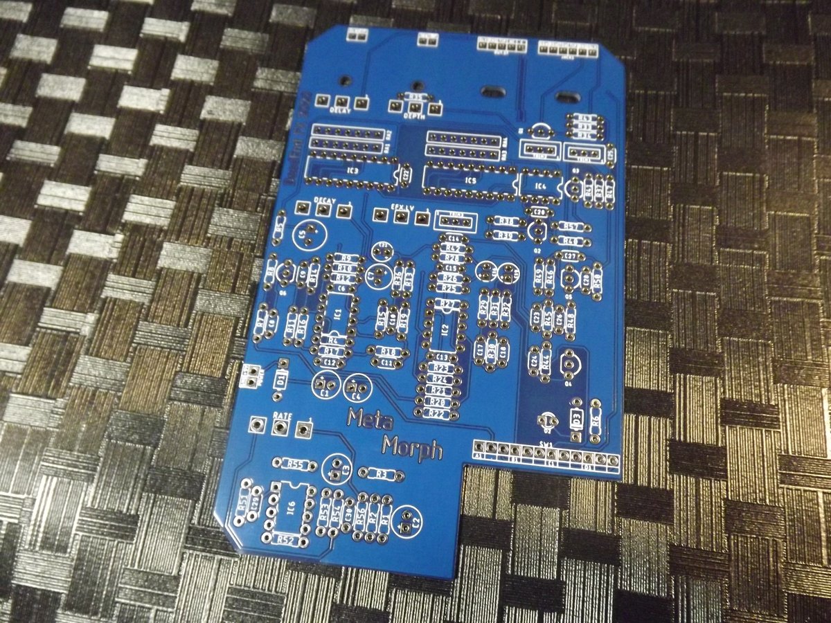
The genesis of this device was some of our customers’ frustration at the ridiculously high price and short supply of MN3011 BBD chips. If you are not familiar, it is an unusual BBD with 6 outputs arranged at specific points along the BBD chain. Using those multiple delay taps in various feedback configurations can make some complex and interesting effects. But the MN3011 has been out of production for many years and there is no current production clone.

serious, genuine, earnest query:
why not reissue a proper MN3011?

is there just not enough demand for it to be feasible?
i'm seeing ....some?


i accept that digital has way more capability and potential and makes more sense to invest into, but perhaps if there were reliable sources, maybe the demand would become induced? - just as we've seen lately with all these new BBD devices - boss DM-101, pastfx's catalog, and anyone else trying to jump on the analog modulation train.
i dunno if any of that would have happened without the reissues.
We looked into building silicon (instead of PCBs) for our CT3101 (MN3101 clone) and the barriers are just too high in many different domains (supply chain, capital investment/payback, technical design, production, quality control and characterization, and on and on). And the 3101 would have been much easier technically since it is a purely digital device -- anyone well versed in VHDL could do the design. But a BBD requires some specialized analog chip design expertise, entirely different than discreet analog. Then the volumes you have to produce just to get into the supply chain (much less at a decent cost point) makes for a very large capital investment. So a year or two and lots of $$ later you have a very specialized, expensive, BBD chip with uncertain market potential. Just could not justify it, which is why I don't think you will see Coolaudio or Xvive or Alfa do it either. You see clones of the 3x05, 07, 09 because they are common devices used in lots of designs. I think the 3011 is just not a big enough market to build new silicon, regardless of the analog versus digital debate.
 
Back
Top