Attempting to breadboard. What is VCC in a schematic?

Barnshart

Member
I would like to try and breadboard the El-Sol (Acapulco Gold) circuit here at home as my first ever breadboard project.

I've already made the PCB and it works fine, I figure it's a simple enough pedal so it might be easiest to breadboard since I already own duplicates of each component.

I'm looking at the schematic from the build doc and I see all kinds of components running to "VCC". I dont know what that is despite Googling it. My understanding is that it would be the + rail on my breadboard, is that correct? Does VCC essentially mean "where the power comes from" ?

Thanks in advance!
 
Also to add to this,

Could somebody please explain how I integrate both sections of the schematic into one cohesive circuit? I see the main schematic for the actual El-Sol portion of the build, and then there is a seperate part of the schematic which I am assuming is simply the footswitch, LED and filtering. But how do I include that in the bread board? Is it even necessary to do on a breadboard?
 
Vcc is the positive supply rail going to ICs, transistors, etc.

Schematic is split in two separate blocks (main circuit and supply) but it's still a single circuit. Just connect the same labels like GND, Vcc, etc.

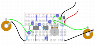
This is how I would breadboard the circuit.

1677047242649.png
 
Vcc is the positive supply rail going to ICs, transistors, etc.

Schematic is split in two separate blocks (main circuit and supply) but it's still a single circuit. Just connect the same labels like GND, Vcc, etc.

This is how I would breadboard the circuit.

View attachment 42583
So on the instance of a breadboard you wouldnt include a footswitch?
 
Correct. I don't use bypass switching when breadboarding. But that's me.

I'll usually stick it in a loop of My Joyo PXL8 and that gets me a footswitch if I need real time comparison but otherwise I'm the same.

For instance, I'm testing a special Fuzz Face buffer right now and I ran the buffer in a loop of the Joyo with a cable from the send of the next loop over to the Fuzz Face. Then I programmed a bank with the buffer bypassed and Fuzz Face loop on, and one with both on so I could switch back and forth in real time to hear my progress.
 
VCC is the input voltage which is filtered and often reverse polarity protected. When you start working with ICs you will often see Vref or Vb or something like that. If you look at the power section of the schematic it will show where that is coming from. IC circuits usually have a pair of voltage divider resistors, usually the same value but not always, with one resistor going from the VCC to the other resistor which goes to ground. Where these resistors meet is Vref, and is used in many circuits as a substitute ground for parts of the circuit. It's usually 1/2 the main operating voltage of the circuit.

Some circuits have more than one Vref. Why? FIIK!
Is Vb the same as Vref?
 
I'm no EE so I could be wrong but my understanding has always been that...

Double letters (Vxx) are power supply voltages, the letter refers to where the voltage is headed (Vcc = collector voltage, Vss = source voltage)
Single letters (Vx) are voltages with reference to ground (Vc = collector to ground, Ve = emitter to ground)
Mixed letters (Vxy) are the voltage between two points (Vbe = base - emitter drop)

Vref would be the stable/constant current for the circuit - "reference voltage."

I think as with all things guitar pedal related, people play pretty fast and loose with the terminology.
 
FWIW, it's probably handy to have some degree of familiarity/consistency with the technical terms to make troubleshooting a problem a bit faster for everyone involved. It's much easier to type, "can you give us Vcc, Vc, Ve?" rather than step by stepping where to put the multimeter probes.
 
Good thread, made me dig up my OLD PedalPower101 doc, which needed refreshing as well as to refresh my understanding (or trying to understand) all the terminology. Here's some of what was in the doc, just the terms and similar to what MDC provided, and I invite corrections/clarifications to the following:


V : Voltage

Va : used to indicate an internal analogue voltage point.

Va alt : anode voltage; Usually seen alongside Vg : grid voltage (now gate voltage) and Vk : cathode voltage. Usually on older (MUCH older circuits! with tubes) but you sometimes see Va,Vk on diodes, e.g. photodiodes​

Vb : Voltage Base (maybe, I’m guessing here)

Vbe : Voltage Base Emitter — voltage between the base and emitter of a BJT

Vc : Collector voltage for a BJT, similarly Ve, Vb may also be used for the emitter and base while Vs, Vd and Vg may be used for the source, drain and gate of FETs. Vc as the actual voltage at the collector

Vcc : VOLTAGE COMMON COLLECTOR positive power supply for many IC's, traditionally this referred to BJT based ICs, the 'cc' referring to the collectors of the integrated transistors. Often this was matched with a negative supply, Vee ('ee' referring to the emitters of the transistors). Vcc is for BJT circuits (c = collector)
Vcc defined as the collector supply voltage (Vc as the actual voltage at the collector).

Vd : Actual voltage at the Drain

Vdd : positive power supply for many IC's, traditionally this referred to FET (NMOS, PMOS, CMOS) based ICs, the 'dd' referring to the drains of the integrated FETs. Often this was matched with a negative supply, Vss ('ss' referring to the sources of the FETs). Vdd is for FET circuits (d = drain)

Vee : negative supply of BJT-based IC, ‘ee' referring to the emitters of the BJT transistors within IC.

Vf : is used to indicate the forward voltage drop of the diode.

Vg :

Vhsys : may be used for the hysteresis voltage of a comparator type circuit.

Vi : input voltage.

Vref : Voltage reference, a precision device designed to maintain an accurate, low noise, constant output voltage. Ideally, the output should remain constant even as parameters, such as ambient temperature, supply voltage, or the load current change.
A voltage reference is a precision device specifically designed to maintain a constant output voltage, even as parameters such as ambient temperature or supply voltage change. The precision of a voltage reference enables its use in several different types of applications beyond a data converter.

Vs : Actual voltage at the Source

Vss : Corresponding negative supply to Vdd, “S” = source.

Vt : May be used for the Thevenin equivalent voltage, or as suggested by WhatRoughBeast the threshold voltage (for a comparator or similar for example), or the termination voltage (also known as Vtt in the case of DDR=type memories).

Vt alt : Voltage threshold​

Vo : Output voltage for op-amps and the like.

Vp : peak voltage (again, for AC) referenced to system ground, or 0V. May also be used for pull-up voltages (which could also be Vpu).

Vpp : peak-to-peak voltage (for AC waveforms), historically this would also be used for the programming voltage for EEPROM or flash memory (particularly those devices that did not generate their own programming voltage on-chip).

Vr : reverse voltage, particularly when referenced to diodes. You may also encounter Vz used to indicate a zener voltage (see above).

0V : Zero-volts, not to be confused with Vo, refers to the system ground. Also,

Additionally...


PEDAL PROTECTION: 1N5817 vs 1N4001
 
Back
Top