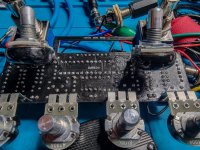
Paragon, 1 Channel no sound..... PLEASE HELP!

aienco

Member
Hello, I went through all the other Paragon threads. I wasn't sure whether to post under those threads or start a new one. I chose the later. Anyway, I have been building electronic kits for 40 odd years and I can mostly resolve the issues with basic troubleshooting even though I am far from an expert..

My Paragon build has a strange issue. At first it was all working fine. Then all of the sudden, Channel one decided it would not work anymore )NO SOUND. The probe just yeilds a buzz no matter what component I touch. I have some weird voltages on the ic's. This is where I am stuck. I am not certain where to look to find the cause of these strange voltages.

D7 voltage is 9.14V

IC1 with ic in.. Without Chip in..
1. 8.27 4.3
2. 8.2 0
3. 8.3 0
4. 16.5 8.7
5. 0 0
6. 0 0
7. 0 4.0
8. 0 0

IC2 with Chip... Without Chip
1. 8.25 4.3
2. 8.27 4.2
3. 8.31 4.3
4. 16.5 8.7
5. 0 8.7
6. 7.31 4.0
7. 8.06 0

IC3 with Chip in..... Without Chip
1. 9.13 8.9
2. 5.5 8.5
3. 0 0
4. 3.0 3.9 keeps going down with probe left on pin 4
5. 2.97 0
6. 4.3 0
7. 5.6 0
8. 9.14 8.9


I hope someone can shed some light on this. I have another board and I am about to give up on this one and start with the new one...

Thanks.. Tony.
 
Sounds like a grounding problem pin 4 on IC1 and 2 should be 0v

You've also omitted the reading for IC2 pin 8

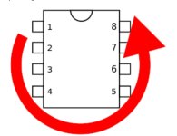
Are your pin numbers correct Ic pin numbers .jpg
 
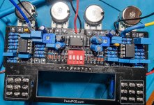
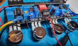
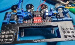
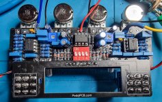
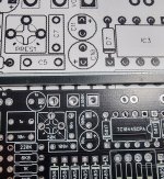
Post some nice clear images so that component value and orientation and wiring can be seen and traced

Pin 4 as you can see in the schematic power section should be 0v ground

You haven't accidentally put the new ICs in upside down?

When you say it was working was it in or out of its enclosure

What voltage do you get at D15 cathode
 
Will do, however I have gone over all the values of components 5 times and re-soldered every connection, all the basic stuff. I will get onto the above.
 
I noticed that on the board layout and the circuit diagram, one specified one way and the board specified the other. Given that it was working, I assumed I had chosen the right one of the two.
 
R12 13 is 8.25V...... This was an Item of confusion... If you look at the board and the paper diagram, you will notice C10 is shown with the positive in different orientations. So I followed the circuit diagram. Or at least I thought I did. I obviously either have the wrong diagram.. Even though I just downloaded it last week, or two boards that have been labeled incorrectly.???? 669.jpg
 
  • Like
Reactions: fig
Looking at the board, the round pad is connected to the ground plane, so that is the -ve terminal of C10, which I think means you have it correct
 
Your capacitors are installed correctly for your revision of the PCB.

Your voltage measurements don't make sense. Pin 4 of IC1 and IC2 should always be 0V, they're connected directly to the ground plane so there's no way they should have any DC voltage at any time.

Pin 8 on the other hand, should measure what you have listed for Pin 4. Are you absolutely sure your pin numbers are correct in the voltage list above?
 
I'd perhaps take voltages again, some are confusing no voltage on either side of D15 for example but voltage beyond it

I down loaded the build doc again just to make sure I was on the right revision I did think maybe a different rev hence me asking rather than saying C10 was wrong

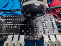
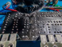
Post a pic of the solder side did you do anything other than change the ICs ie reflow joints etc
 
that is how I measure the chips. I know the way they run. However i could have made a mistake. I will re measure just to be safe.

Reflowed joints a couple of times actually. Cleaned the board with board cleaner and checked joints under magnifying glass. Doesn't mean there isn't a problem, but I have tried to eliminate things.
 
Last edited:
Initially I thought it was maybe a solder bridge causing funky voltages I've had the exact same strange readings on a build

Voltages were fine with the IC out of socket and weird in socket it turned out to be a solder bridge which only became active with the IC inserted

If you haven't already have a look at the solder side under magnification to see if there are any bridges etc in my case it was a very thin whisp of solder causing a bridge that took forever to find
 
Here are the latest lot of figures. It appears there were some errors. However the numbers still don't seem correct.

IC 1
1. 8.0
2. 8.0
3. 7.3
4. 0
5. 8.25
6. 8.2
7. 8.3
8. 16.5

IC2
1. 8.0
2. 7.9
3. 7.2
4. 0
5. 8.2
6. 8.2
7. 8.3
8. 16.5

IC3
1. 9.1
2. 5.5
3. 0
4. - (negative) 3.0
5. - 2.9
6. -4.3
7. -5.6
8 +9.1

7-10-1.jpg 7-10-2.jpg 7-10-3.jpg
 
Back
Top