PCB Design Tube Pedal

Hi everyone,

I've got pretty obsessed with diy pedals over the last two years, and I ventured into tube pedals only recently. I've built the Matchless Hotbox, a JTM45 Preamp, and a clone of the kingsley page on veroboards and they all turned out great. However, I recently went down the rabbit hole to create pcbs (for my transistor projects), and I would like to try that for my tube builds as well.
However, my knowledge when it comes to routing and spacing is limited, and i want to avoid any issues with high voltages etc. Does anybody have any advice on that?
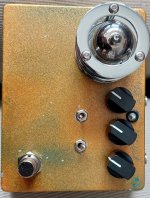
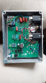
Attached is my attempt at a page PCB. Routing width is 30mil and minimum spacing 16mil.

Bildschirmfoto 2024-04-05 um 12.26.59.png Bildschirmfoto 2024-04-05 um 12.28.43.png
Any help is greatly appreciated. Thanks in advance.

Markus.
 
30mil trace width is very large for a board of any complexity and it's going to get crowded fast. 16mils is plenty of space to avoid arcs at typical preamp voltage, but it's not enough to avoid crosstalk in sensitive and/or high-gain traces.

My recommendation would be to make the traces thinner and spread them out more. When I design tube pedals (I've done a handful now) I typically do 40mil traces for the heater rail (high current) and the main power signals on the HV supply, then 12-15mil (depending on how crowded the board is) for everything else. On REALLY simple boards I'll go up to a 20mil trace for signals, but I never go larger than that.

One caveat is that I typically do 4-layer boards so I have a dedicated ground layer and a split power layer that carries all the VIN and HV, and that helps a lot both in keeping the board uncluttered and in keeping the noise floor low.
 
Thanks so much. I was hoping you were going to reply @vigilante398 :) I built three of your boards so far and they are all amazing (Ambassador, Diplomat, and King Nothing).

I'll definitely adjust the routing width accordingly. In my attempts above I tried to move all power supply components on one section of the board and the rest on the other side - however not sure whether this is sufficient to avoid noise and crosstalk. Do you think this is doable with 2 layers?

I am not sure whether I understand you correctly on how you split the layers. 1 layer for the signal path, 1 layer for power supply and heater supply, and 1 ground layer? That would leave on layer in case it is a larger layout?

And one more question: if you would include an output buffer e.g. with a lnd150 hv-mosfet, do you think it is important to decouple the HV for the valve(s) and the mosfet?

thanks again!
Anything can be made on a 2-layer board if the board is big enough and you're patient enough with routing. But your main concern isn't going to be crosstalk between power and audio signals, it's crosstalk between audio signals and other audio signals. You can route audio signals 10mil away from your HV rail all day and it will be fine. AC signals (like audio) like having a DC reference to keep noise down, it doesn't have to be ground. But if you route your input line too close to your output line, you're going to have very significant problems with noise and possibly oscillation, depending on the gain of the circuit.

My 4-layer layouts are always
  • top layer - signal
  • internal 1 - ground
  • internal 2 - split power
  • bottom layer - also signal
If you're trying to run all of your signal traces on one layer you're going to have a hard time getting things to fit.

If you're doing a FET output I would say it's not a bad idea to have an additional filtering stage between the tube's HV line and the FET's HV line, but I don't think I would say it's critical.
 
Hey guys, just to report back. I largely followed Nathan's advice and ordered my first tube pcbs from jlcpcb. It arrived petty quickly and was an easy bulld. It is a Page clone, but I reworked the Design from above. It sounds great, no noise whatsoever. Pics below.
 

Attachments

  • 20240420_140622.jpg
    20240420_140622.jpg
    318.9 KB · Views: 42
  • 20240420_140616.jpg
    20240420_140616.jpg
    921.9 KB · Views: 42
Thanks so much. I was hoping you were going to reply @vigilante398 :) I built three of your boards so far and they are all amazing (Ambassador, Diplomat, and King Nothing).

I'll definitely adjust the routing width accordingly. In my attempts above I tried to move all power supply components on one section of the board and the rest on the other side - however not sure whether this is sufficient to avoid noise and crosstalk. Do you think this is doable with 2 layers?

I am not sure whether I understand you correctly on how you split the layers. 1 layer for the signal path, 1 layer for power supply and heater supply, and 1 ground layer? That would leave on layer in case it is a larger layout?

And one more question: if you would include an output buffer e.g. with a lnd150 hv-mosfet, do you think it is important to decouple the HV for the valve(s) and the mosfet?

thanks again!
@vigilante398 i didn't realize sushi box fx was yours, going to check that out. really cool thread, i aspire to pcb design within the next year.

thanks for the details guys!
 
Back
Top