5TH "Test" program on FV-1 chip solution? (will this work?)

BrooksBlackhawk

New member
I thought of a potential solution to the blank 5TH "Test" program on FV-1 chip. Like the arachnid but the focus being on the internal programs but with one bonus program on the the external eprom and no additional switch needed to access it.

We know that:
"ROM Programs
The FV-1 includes 8 programs in the internal ROM, these programs and the assigned potentiometer input controls are detailed in Table 1.

Table 1 - ROM Programs
Prg # Description POT0 POT1 POT2
0 Chorus-reverb Reverb mix Chorus rate Chorus mix
1 Flange-reverb Reverb mix Flange rate Flange mix
2 Tremolo-reverb Reverb mix Tremolo rate Tremolo mix
3 Pitch shift Pitch +/-4 semitones - -
4 Pitch-echo Pitch shift Echo delay Echo mix
5 Test - - -
6 Reverb 1 Reverb time HF filter LF filter
7 Reverb 2 Reverb time HF filter LF filter"

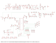
So for the 5th program, if the switch sent pin 13 high (3.3v) the external eprom kicks in right?

SEE SW_2 AT BOTTOM OF SCHEMATIC


BROOKS BLACKHAWK
 

Attachments

  • MULTI FX FV-1 SMD.pdf
    41.8 KB · Views: 6
  • MULTI FX FV-1 SMD.png
    MULTI FX FV-1 SMD.png
    564.3 KB · Views: 10
TBH, I don't think the 5th 'Test' patch in the internal FV-1 patches was ever a problem to be solved. Rather the entire set of patches internal to the FV-1 were originally planned as "test" patches and patch #5 is just a "pass-through' patch for testing and evaluation like all the other internal programs. And in my POV, employing an external EEPROM with only one patch on it (to circumvent the singular 5th internal FV-1 patch) is like driving an 8 passenger vehicle around but never having any passengers. After all, if using an external EEPROM at all, why not just also use a complete custom set of patches and utilize the entirety of the external EEPROM and never hassle with the internal programs at all?

Further, it's not a good idea to tie pin 13 of the FV-1 directly to +3.3V. Rather it is a best practice to pull pin 13 up thru a 10K resistor for accessing an external EEPROM. With pin 13 pulled high thru a 10K resistor, the internal programs can then safely be accessed by connecting pin 13 directly to ground.

I guess I fail to see the advantage in your supposition.
 
This should work, but what you'll end up with is a PCB that can only access the internal programs and a single program from an external EEPROM.

I know, I know, that was the goal... but...

What I would recommend instead is just loading the seven internal programs onto an EEPROM along with an additional program of your choice into patch #5. Now you have access to all of the internal programs, and the ability to switch to another full set of eight just by swapping out the EEPROM.

Exact same BOM, but more flexibility.

All of the internal programs are available in SPN format on the SpinSemi website:
 
I forget where l had seen it but I remember reading somewhere someone claiming they had figured out how to re program the internal algorithms.
That would be an interesting read. Please share the link if you find it again.

Although TBH, I don't think reprogramming the internal patches is possible because there is no direct access to the internal ROM.
 
That would be an interesting read. Please share the link if you find it again.

Although TBH, I don't think reprogramming the internal patches is possible because there is no direct access to the internal ROM.
I came across it when I was figuring out how I was going to designing the dual eeprom board I did, I vaguely remember some talking about it, I looked at so many threads and forums I couldn’t even begin to remember where that was… but in some corner of the internet it’s there whether they were actually able to do it or not, I wasn’t that interested in figuring that out, personally, I’m kind of over that deep end of the fv-1 rabbit whole for now. This seemed like it might be interesting to someone looking at this thread… happy hunting.
 
TBH, I don't think the 5th 'Test' patch in the internal FV-1 patches was ever a problem to be solved. Rather the entire set of patches internal to the FV-1 were originally planned as "test" patches and patch #5 is just a "pass-through' patch for testing and evaluation like all the other internal programs. And in my POV, employing an external EEPROM with only one patch on it (to circumvent the singular 5th internal FV-1 patch) is like driving an 8 passenger vehicle around but never having any passengers. After all, if using an external EEPROM at all, why not just also use a complete custom set of patches and utilize the entirety of the external EEPROM and never hassle with the internal programs at all?

Further, it's not a good idea to tie pin 13 of the FV-1 directly to +3.3V. Rather it is a best practice to pull pin 13 up thru a 10K resistor for accessing an external EEPROM. With pin 13 pulled high thru a 10K resistor, the internal programs can then safely be accessed by connecting pin 13 directly to ground.

I guess I fail to see the advantage in your supposition.
Well, everything after "further" was useful. Thanks for your input.
 
This should work, but what you'll end up with is a PCB that can only access the internal programs and a single program from an external EEPROM.

I know, I know, that was the goal... but...

What I would recommend instead is just loading the seven internal programs onto an EEPROM along with an additional program of your choice into patch #5. Now you have access to all of the internal programs, and the ability to switch to another full set of eight just by swapping out the EEPROM.

Exact same BOM, but more flexibility.

All of the internal programs are available in SPN format on the SpinSemi website:
Thats a great point, also, I can just put an internal/external memory switch or even better have it be a foot switch that can toggle to another patch.
 
You can. You could toggle between two separate EEPROMs as well.
Could this effectively be done with a 4PDT switch or should there be other components (other than 2 - 8 pin sockets on a daughterboard) to reduce the strain from sudden switching?
 
You can do it with an SPDT. You don't have to hot swap the EEPROM, you connect them in parallel and toggle one of the address pins of the EEPROMs to effectively disable one or the other.

With an SPDT you have to change to another program before the newly selected EEPROM is loaded.

You can use a DPDT and toggle the Int/Ext pin simultaneously to instantly swap to the new EEPROM.

There is a schematic here somewhere on the forum showing how to do both.
 
I
Thats a great point, also, I can just put an internal/external memory switch or even better have it be a foot switch that can toggle to another patch.
I did something like this and posted the schematic I used it works really well and programs switch when switching banks if you incorporate the internal algorithms with the two EEPROMs.

 
I

I did something like this and posted the schematic I used it works really well and programs switch when switching banks if you incorporate the internal algorithms with the two EEPROMs.

I found it! Thanks!
 
You can do it with an SPDT. You don't have to hot swap the EEPROM, you connect them in parallel and toggle one of the address pins of the EEPROMs to effectively disable one or the other.

With an SPDT you have to change to another program before the newly selected EEPROM is loaded.

You can use a DPDT and toggle the Int/Ext pin simultaneously to instantly swap to the new EEPROM.

There is a schematic here somewhere on the forum showing how to do both.
Is there a way to "trick" the FV1 into thinking a new program has been selected when swapping between the EEPROMS without actually changing programs? I would like to be able to swapped to a new chip without having to toggle a new program to get it to recognize it. I'm working on a build that has 4 chips to move between on a 2P4T, and I'm hoping I can use the extra pole to achieve this somehow. I've been hacking away at some boards for a few days now, and can't for the life of me come up with anything that works.
 

Attachments

  • Schematic_MULTIEEPROM_2024-02-04.pdf
    68.3 KB · Views: 2
Yes, look at the schematic in the first post of @Paradox916 thread.

You use a DPDT to switch the EEPROM and briefly pulse the Int/Ext pin.
 
Yes, look at the schematic in the first post of @Paradox916 thread.

You use a DPDT to switch the EEPROM and briefly pulse the Int/Ext pin.
In this case, doesn't this only work because you are switching to the internal programs? I am trying to find a way to do so without including the programs stored in the chip. My understanding is that the 3 positions on the toggle in this schematic goes: 1st EEPROM-Internal Algorithms-2nd EEPROM. I guess my question is "Is it possible to achieve this function without switching to the internal programs at all, and strictly read external codes?".

EDIT: Just tested it, and it worked! My original understanding was that this only worked because of the physical switching between external/internal. I didn't realize that the pulse was in fact enough to make this happen. I will start designing now. Thanks for the help!
 
Last edited:
I don't think the FV-1 will automatically recognize a fresh EEPROM when one is hot-swapped. Something has has to re-trigger the FV-1 to read the patch at the current memory address. Briefly toggling the internal patches will certainly do that. But to get that to happen with external EEPROM hot-swapping, something needs to trigger the FV-1 to do so. It seems any brief address change or pulsing pin 13 would suffice.
 
Last edited:
Yes, look at the schematic in the first post of @Paradox916 thread.

You use a DPDT to switch the EEPROM and briefly pulse the Int/Ext pin.
What do you think of something like this?
 

Attachments

  • eeprom2.png
    eeprom2.png
    183.9 KB · Views: 7
I don't thin the FV-1 will automatically recognize a fresh EEPROM when one is hot-swapped. Something has has to re-trigger the FV-1 to read the patch at the current memory address. Briefly toggling the internal patches will certainly do that. But to get that to happen with external EEPROM hot-swapping, something needs to trigger the FV-1 to do so. It seems any brief address change or pulsing pin 13 would suffice.
It seems to be doing the trick. I won't know fully until I can have both functions on one switch. The schematic I just posted above is how I plan on laying it out at the moment.
 
Back
Top