Chauffeur Overdrive build HELP. (Pictures added)

marcusbig

New member
Hi All

I've been working on the Chauffeur Overdrive as my first pedal build.

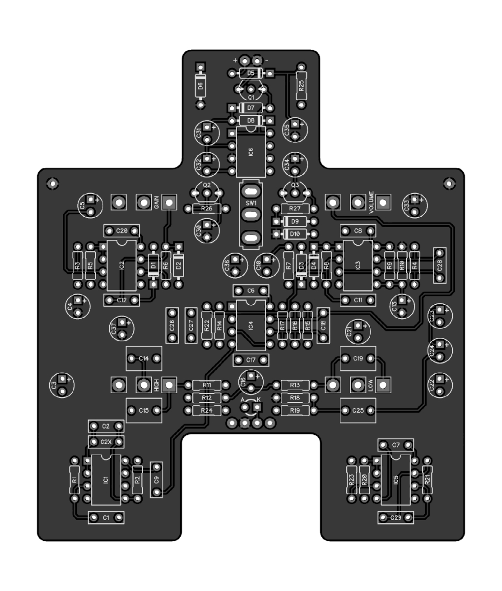
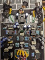
First of all, the inspection of all the parts and the PCB.
Fortunately, I found that one of the PCB patterns is disconnected in the middle of the line between R13 - IC4 6pin (faulty PCB). Anyway, so I patched it up with a wire.

When I turn the pedal off (LED off), I can get sound through the amp (bypass mode).
However, when I turn the pedal ON (LED is ON), I do not get any sound through the amp. Just quiet (no hum) Even if controlled the 4 knobs, nothing changes.

Does anyone have experience with this kind of problem? Or know how to fix it?
Before I give up, I just want to hear someone's technical opinion.

I will be grateful for any help you can provide. (y)
Cheers. Marcus.

Chauffeur_Front.JPG Chauffeur_Back.JPG
 
Solution
Found the problem. Awesome tone :LOL:

[Replaced parts]
1. C4 - Electrolytic capacitor 47uF. (Faulty)
2. Q100, Q101 - 2N4401 NPN TR (Looks OK but just in case)
3. Q102 - 2N4403 PNP TR (Looks OK but just in case)

[Jump Wire]
There is a connection issue between the gain switch and the PCB pattern for C4 due to disconnection.

Special thanks to @music6000 and @comradehoser (y) your guys inspired me.
I appreciate it.

1706534063185.png 1706534227670.png
R13 pad connects to IC4 Pin 7, not 6.
It would have been way better to run a piece of insulated wire from R13 Pad to Pin 7 or R14 pad.
You have made a bit of a mess joining it & may have Grounded it,
This is not a project for a first Build.
If I 'm being honest, the wiring is not very good, exposed wire is not good!
My apologies, the R13 pad is connected to IC4 pin 7.
Thank you for your comment.
 
Fortunately, I found that one of the PCB patterns is disconnected in the middle of the line between R13 - IC4 6pin (faulty PCB). Anyway, so I patched it up with a wire.
This current PCB has been successfully Built so it's strange that you say the Trace was missing!???
 
I don't see the jumper between r13 and ic4 pin 7. If you originally tested to pin 6, and didn't have continuity, you may have jumpered in error. You could always remove the jumper and see what's what.

What I do see is c11 is very melted. If it's to the core, it might render the capacitor inoperative. Ask me how I know! That might affect your output right there.

In any case, a useful thing to do in this case, besides 1) visual inspection of component orientation, 2) testing between all points of the circuit for continuity and 3) ascertaining the voltages of the current in and all pins of the transistors and ICs is to do an audio probe. Follow the signal in along the schematic and see where it stops or attenuates. That's the problem there.

It could help also if the photos were a bit more focused and less blurry. I can't really tell what's going on with your switch wiring in the first photo. Off board wiring errors, breaks, and shorts/groundings are often the cause of dead signal for me.
 
Need the Voltages on all 5 IC's?

Op Amp Direction.jpg
I don't see the jumper between r13 and ic4 pin 7. If you originally tested to pin 6, and didn't have continuity, you may have jumpered in error. You could always remove the jumper and see what's what.

What I do see is c11 is very melted. If it's to the core, it might render the capacitor inoperative. Ask me how I know! That might affect your output right there.

In any case, a useful thing to do in this case, besides 1) visual inspection of component orientation, 2) testing between all points of the circuit for continuity and 3) ascertaining the voltages of the current in and all pins of the transistors and ICs is to do an audio probe. Follow the signal in along the schematic and see where it stops or attenuates. That's the problem there.

It could help also if the photos were a bit more focused and less blurry. I can't really tell what's going on with your switch wiring in the first photo. Off board wiring errors, breaks, and shorts/groundings are often the cause of dead signal for me.
The jumper is there above the LED on the back of the PCB above in the picture!
 
I don't see the jumper between r13 and ic4 pin 7. If you originally tested to pin 6, and didn't have continuity, you may have jumpered in error. You could always remove the jumper and see what's what.

What I do see is c11 is very melted. If it's to the core, it might render the capacitor inoperative. Ask me how I know! That might affect your output right there.

In any case, a useful thing to do in this case, besides 1) visual inspection of component orientation, 2) testing between all points of the circuit for continuity and 3) ascertaining the voltages of the current in and all pins of the transistors and ICs is to do an audio probe. Follow the signal in along the schematic and see where it stops or attenuates. That's the problem there.

It could help also if the photos were a bit more focused and less blurry. I can't really tell what's going on with your switch wiring in the first photo. Off board wiring errors, breaks, and shorts/groundings are often the cause of dead signal for me.

First of all, appreciate all your comments. (y)

1. Jumper between R13 and IC4 pin7
1706025260009.png

2. C11 is very melted - Yes. accidentally touched by Soldering Irons (But before melted sound was not coming out from the pedal)
1706026383107.png

3. Visual inspection of component orientation --> Couple of times already since last week.
4. Testing between all points of the circuit for continuity --> Couple of times already since last week.
5. Ascertaining the voltages of the current in and all pins of the transistors & ICs
--> I have Digitech multimeter but honestly don't know how to do it. (I'm sorry for my limited knowledge) :cry:
6. Detail photo - Attached (Photo-001.jpg)
 

Attachments

  • Photo-001.jpg
    Photo-001.jpg
    586.9 KB · Views: 3
I am confused. I was expecting to see something between r13 and ic4 pin 7. I thought that was a hair or something. marcusbig is jumpering one pad of r13 to the other?

[edit: wrote before reading new messages. I see, now with the new pic. How did you know where to place it? Was it accidentally cut or visibly damaged? If the trace was bad, I would jumper from one pad to the other with a wire, not in the middle of the trace unless there's a distinct area of damage. Is the jumper joined to the trace underneath the pcb coating?

My limited experience with melting film caps leads me to believe that C11 is toast. A little melt is okay. Once I see metal, I suspect not. Mine was not, and I had to replace it to get the pedal to work.

How to test voltages: hook up the board and your black probe to a ground, (usually I mount at least the in jack to the outside of an enclosure and put the black probe in the screw hole--but you could connect the sleeve to an enclosure with a an alligator clip cable--maybe you can even just connect it to a board ground), plug in the board, set your probe to auto V, and touch the component legs, you should get readings. Mind that some will read positive and others negative, some will also just read 0 or close to it, it's normal.
 
Last edited:
You have to measure every Pin as numbered above on 5 IC's.
You should have around 9v on Pin 8, that's where power is going in, Pin 4 is ground so you will not get a reading, it will be in mw.
Pins 1, 2 ,3, 5, 6, 7 should be 4.5v or slightly more.
 
You have to measure every Pin as numbered above on 5 IC's.
You should have around 9v on Pin 8, that's where power is going in, Pin 4 is ground so you will not get a reading, it will be in mw.
Pins 1, 2 ,3, 5, 6, 7 should be 4.5v or slightly more.
Thanks a lot for your guidance. Here are the results of the test. - (Note) 3 times average value.
Please see picture below.

[Observation]
1. IC2 pin1, 2 & 3 voltage is keep changing between 200 ~ 300mW.(Almost No voltage detection)
2. IC2 pin 6 voltage 4.61 Volt
2. IC100 - 7660SCPAZ (Charge Pump IC) pin 5 voltage is Negative(-) 4.99V

1706107856864.png
 
Back
Top