Procrastinator refuses to work........

Ariosto

Member
Hello everybody,

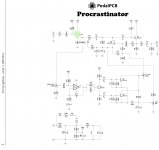
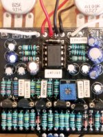
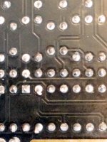
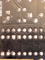
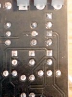
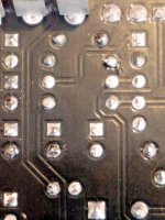
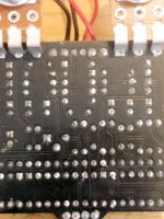
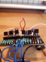
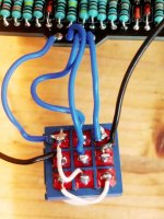
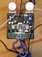
I finished to assembly this pedal yesterday, but I am having a strange trouble and maybe here there is someone who could help me. As the title says, it don´t want to work -that means, in the bypass mode there is no problem, and no sound when engaged-. Well, I checked every component before soldering, looked for cold joints as well (it´s now too late and I´m tired, but I promise to upload some pictures tomorrow) and now I am trying to find something with an audio probe. The signal "dies" in a very early stage of the circuit (Q1), is that not rare? Maybe someone with more knowledge that me could give me some hint.

Thanks in advance,

Ariosto.
 

Attachments

  • Procrastinator-3.jpg
    Procrastinator-3.jpg
    369.6 KB · Views: 14
Photos would be a good idea. It would also be useful if you can post voltages. The pins of the op amp would be useful, and the voltages of Q1 (and other transistors as well) would be good. If the signal is only getting to Q1 it is quite likely that it is not getting correct power.
 
Photos would be a good idea. It would also be useful if you can post voltages. The pins of the op amp would be useful, and the voltages of Q1 (and other transistors as well) would be good. If the signal is only getting to Q1 it is quite likely that it is not getting correct power.
Thank you for the quick response! Here the pictures, and later I will measure voltages:
 

Attachments

  • 01.jpg
    01.jpg
    789.6 KB · Views: 24
  • 02.jpg
    02.jpg
    736.8 KB · Views: 21
  • 03.jpg
    03.jpg
    788.2 KB · Views: 17
  • 04.jpg
    04.jpg
    622.3 KB · Views: 16
  • 05.jpg
    05.jpg
    757.7 KB · Views: 18
  • 06.jpg
    06.jpg
    779.3 KB · Views: 23
  • 07.jpg
    07.jpg
    523.2 KB · Views: 20
  • 08.jpg
    08.jpg
    1.2 MB · Views: 20
  • 09.jpg
    09.jpg
    862.9 KB · Views: 24
  • Procrastinator.pdf
    500.8 KB · Views: 10
One end of r101 joins to one end of r102. Can you measure the voltage at that point.

Also, can you give us all 3 pins for each transistor?
 
One end of r101 joins to one end of r102. Can you measure the voltage at that point.

Also, can you give us all 3 pins for each transistor?
Ok, here I go:

Q1: 1: 0.01 2: 0.02 3: 0
Q2: 1: 0.01 2: 0 3: 0.01
Q3: 1: 8.19 2: 3.59 3: 5.63
Q4: 1: 0.01 2: 0.90 3: 0.61
Q5: 1: 0.01 2: 0 3: 0
Q6: 1: 0.01 2: 0 3: 0

Voltage between R101 and R102 0 0.01


Hope that it would be useful.
 
Question: Are the jack tips soldered to the switch or to the pcb?
As start, I connected the jacks direct to the PCB (without switch) and I didn´t have no signal. I connected the switch already (see picture above), and the signal goes out to amp when off, but nothing at all when engaged.
 
The reason I ask is, you have white from the pcb and black from the switch (this may just be your preference), but I am pretty sure the tip needs to be wired to the switch.
 
The reason I ask is, you have white from the pcb and black from the switch (this may just be your preference), but I am pretty sure the tip needs to be wired to the switch.
The white cables are grounds (in both plugs) and are connected to the PCB. The black ones (either in both plugs) go to the tips and are soldered to the switch in the middle row eah one to the sides. I followed the instruction in the official PDF.
 
  • Like
Reactions: fig
The white cables are grounds (in both plugs) and are connected to the PCB. The black ones (either in both plugs) go to the tips and are soldered to the switch in the middle row eah one to the sides. I followed the instruction in the official PDF.
Otherwise I think it won´t never work on bypass like it does.
 
  • Like
Reactions: fig
Did you sub the 2sk30 for another jfet? 2sk30 have a weird pinout and your pic is too blurry for me to see . On my build I had sound when engaged but the trimpot didn't work for biasing the swell. To help I socketed r23 and tried a lower value and solved pretty much all my problems :p it's not the same issue I know but if you do get pass your problem and the swelling does not work try this ^^
 
PJS has pointed you in the right direction

Looking at your voltages VCC is 8.19v going up to Q3 collector so at the voltage divider junction R101 and 102 you'd expect half of that (VREF) with yours at 0.01v it won't bias your op amp or transistors correctly

You should also have 8.19v going into the top side of R101

Try reflowing R101, 102 and C101 solder joints just hold your iron on them for around 4 seconds until you get a nice flow of solder and a good connection between pad and component legs then recheck your VREF voltages
 
Ok, I think I´ve got some 2SK30 anywhere around. That would be the first failure to check, and the second is making a better soldering contact in the resistors 101 and 102. I´ll try them both and then I´ll write a report about it.
 
The other thing is that you may have a short between your Vref and ground somewhere on the board. Once you have done the checks that Mcknib has suggested, if it still has essentially 0V at Vref then check every Vref trace for a potential short carefully. If there are none then there may be a bad component shorting those two together.
 
Although I don't think your transistors are the problem it's not beyond the realms of possibility, a quick check to see if your IC or transistors are causing any problems rather than change them, is to check your VREF points with them out of socket and check voltages on the empty sockets at IC pin 3 or Q1 middle base pin
 
Although I don't think your transistors are the problem it's not beyond the realms of possibility, a quick check to see if your IC or transistors are causing any problems rather than change them, is to check your VREF points with them out of socket and check voltages on the empty sockets at IC pin 3 or Q1 middle base pin
NOOB QUESTION:

Whar are the "VREF points"?
 

Attachments

  • index.jpg
    index.jpg
    12.1 KB · Views: 0
Sorry I should have mentioned labelled on the schematic I'm forgetting you're new to this

You'll see a few labels on schematics showing references like VREF, VCC etc

VREF or sometimes VB, Vbias, VR is usually the bias voltage commonly half the power supply (VCC) all voltages are usually referenced to ground 0v for measuring purposes

Very handy when debugging because it shows you where to expect these voltages

If you look at the bottom right of the schematic you'll see the power supply section where you can see power going in at the + sign through D100 the polarity protection diode which prevents circuit damage if you use an incorrect polarity power supply C100 filters any voltage ripple to ground to prevent any unwanted noise getting into your circuit and being amplified etc

The power in will be whatever your supply puts out from your voltages it looks like 8.45v you'd drop around 0.26v through the diode giving you your 8.19v going into your circuit at VCC eg Q3 collector pin 1 where you'll see the VCC label so all VCC labels should be around 8.19v less a little voltage drop through resistors, diodes etc

If you follow the power section along you can see it goes to R101 and 102 which form your voltage divider they are both the same value so would divide your voltage equally half of your 8.19v so 4.09v giving you your VREF

You should then expect around that voltage at your VREF points labelled on the schematic less a little voltage drop as before, if as in your case you're not getting that then you would check visually for correct component values, polarity etc then as you have measure voltages to help track down the source of the problem

From PJSs advice we know your problem is around the voltage divider or something connected to it

All points with the same label are electrically connected so if you continuity check any points with the same label you should get a connection

All little points you can use to help with your troubleshooting
 
Last edited:
Back
Top Bottom