Quick Schematic Flow Question...

Ginsly

Well-known member
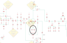
In an effort not to pester Buddy any further, figured I'd post this quickie. Trying to lay out my first Vero, and it's revealing gaps in my schematic knowledge. Here's a chunk I'm wondering about:
Screen Shot 2024-12-26 at 7.59.37 PM.png
I mistakenly thought that I could simply connect C2 to Q2's collector, and since R4 connects the base and collector that would kinda connect everything that needs to be in contact.

Wrong!

First off, the connection point and path to Base right after C2 indicates that it needs direct contact with Q2's base evidently. From there I'm a little confused.

I actually took a look at the pcb traces for this circuit, and it looks like C2 is ONLY connected to Q2's base, and not to the collector as well like I thought. R4 is between them on the schematic, and instead of connecting C2 to Q2's collector, it looks like it's simply connecting base and collector.

Is that correct? C2 connects to Base only and R4 connects Base and Collector?
 
Correct
R4 and C2 share a common node of Q2-B
Edit to add
I was taught to look at a schematic as nodes. Everything that touches Q2-B shares a node, no matter how it connects. Trace, wire etc. same and common node. R4, C5, R6 and Q2-C are a common node. As long as they all connect and don't connect with anything else, you're good.
Thank you! The "nodes" tip clears a lot of things up, and looking at it that way there is absolutely no connection between C2 and collector. Great advice, this will help immensely going forward.

Speaking of which, I just plucked C2's link to collector on the breadboard and the whole thing came to life. No wonder it sounded so... awful. Now it sounds awful in the correct way. :)
It really helps and I can imagine in doing strip/vero layouts(I don't mess with them much) it would be a good way to look at it.
It is beneficial when probing as well.
 
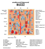
@jwin615 maybe you can humor me for a sec, as I’m comparing some schematics to stripboard and trying to clear some things up. This is a snapshot of part of a Smallsound/Bigsound Buzzz, slightly modified by DEFX. The stripboard layout has C7 and C8 linking directly to Q2’s emitter, but in the schematic they don’t share a node with Q2. There’s nothing between them however, so they must link directly to the emitter even though it’s a coupla nodes away. I just assumed that in order to connect directly you had to share one node, but in some cases more than one node is involved…right? Ok I have to stop saying “node” now.
1735366549128.jpeg
1735366579016.jpeg
 
Last edited:
C7 and C8 connect to Q2's emitter, not the base. (Row N)
My mistake, that’s what I meant! Thanks for the heads up. Edited.

So even though they don’t share a direct node with Q2’s emitter in the schematic they do indeed link directly to it in practice?
 
Note Q1 collector shares a common node(blue) with R9, C5 and Q2-B. Even though R9 and C5 appear "between" the two BJTs, there is nothing actually between them. All a common node.
 
R10, R11, C7, C8 are have one point in series to the emitter and parallel to the other components(on one end).
I think part of what was confusing me was the “extra” node that DEFX puts at the emitter of each transistor (with a little red/green box)- why is that?

Note Q1 collector shares a common node(blue) with R9, C5 and Q2-B. Even though R9 and C5 appear "between" the two BJTs, there is nothing actually between them. All a common node.
Gotcha! Your common node highlights helped a lot, makes much more sense now. Thank you!!
 
Last edited:
I think part of what was confusing me was the “extra” node that DEFX puts at the emitter of each transistor (with a little red/green box)- why is that?
Laziness/failure to clean up the schem? Or maybe there's a test point there?
It's inconsequential, regardless.
 
So are C7 & C8 10nF or 10uF? Is that a mod? Or a typo? 10 nano 'lectro's? 10nF doesnt make much sense..
Pretty sure it's a mistake, and should be 10uF (this is from the DBL blog, btw). Seems like most of his layouts are solid, but this one has a few changes that I don't quite understand. For instance, the 100nf cap in the lower middle of that snapshot is supposed to be 220nf, based on DEFX's schematic. DBL omitted his Buzzz mods, but I doubt it has anything to do with that. Strange.
 
I think part of what was confusing me was the “extra” node that DEFX puts at the emitter of each transistor (with a little red/green box)- why is that?

BJT-MULTI-NPN, does this footprint have an extra pad to accommodate different pinouts?

If so, that little red "loop" is a connection between two pins. (For example, the two Emitter pins in the pic below)

The green point that sticks off is the additional Emitter pin.


1735400216117.png
 
BJT-MULTI-NPN, does this footprint have an extra pad to accommodate different pinouts?

If so, that little red "loop" is a connection between two pins. (For example, the two Emitter pins in the pic below)

The green point that sticks off is the additional Emitter pin.


View attachment 87795
Ah! Ok that makes sense! Couldn't for the life of me figure out what that meant.
 
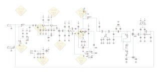
Revisiting the Buzzz/Zuperbee and starting to breadboard it - there are still some odd things I don't understand about the schematic, though. What is going on with this floating chunk placed under (but not connected to) Q4 and Q5? All of the little "C2", "C3", etc flags are a little confusing too, but I assume that has more to do with the pcb layout itself..?
Screen Shot 2026-01-11 at 12.15.34 PM.png
 
Generally those little flags represent connections. So that C2 flag looks like it connects to the other one directly north of it on the schematic where it says GAINSW_A being one side of a toggle for something or other
 
Generally those little flags represent connections. So that C2 flag looks like it connects to the other one directly north of it on the schematic where it says GAINSW_A being one side of a toggle for something or other
Ahhh that toggle at the top is involved... ok that makes sense. It's odd that the switch is linked to the collectors even though it seems to be taking an emitter resistor and bypass cap in or out of the circuit... it's probably changing more than that, though. Thanks for the tip HK, much appreciated. I'll take a closer look at the whole schematic in comparison to the stripboard layout - that helps clear things up sometimes. (The DEFX schematic doesn't match the vero layout exactly, as the DBL version omits the trim pot and Q6 Starve jumper.)
Zuperbee build doc_opt.jpg
Screen Shot 2026-01-11 at 2.25.57 PM.png
 
Last edited:
Back
Top